Page 18 - Chip Scale Review_November-December_2023-digital
P. 18
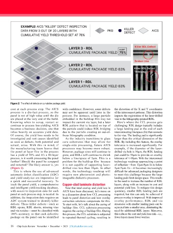
Figure 2: The effect of defects on cumulative package yield.
        cost at each process step. The AICS   with confidence. However, some defects   the distortion of the X and Y coordinates
        process is a die-last process, so the   may not be apparent until later in the   of the interconnect patterns. This distortion
        panel is not of high value until the die   process. For instance, a large particle   impacts the registration of the laser-drilled
        are placed at the very end of the build.   embedded in the build-up film may not   vias to the lithography-printed RDL.
        Knowing when to scrap, restart or   impact the current via layer, but a later   Here’s where the CCL process gets
        continue to process low-yielding AICS   RDL pattern that is located on top of   challenging: RDL design typically includes
        becomes a business decision, one that   the particle could induce RDL bridging   a large landing pad at the end of each
        relies heavily on accurate yield data.   due to the particle creating an out-of-  interconnecting line/space (l/s) that connects
        Of course, the yield loss needs to be   focus lithography condition.  to the vias. The landing pad is significantly
        investigated and root causes identified   As the industry transitions to glass   larger than the critical dimension of the
        as soon as defects, both potential and   core substrates that may allow for   RDL. By including this feature, the overlay
        actual, arise. With this in mind, if   single-side processing, future AICS   tolerance is increased significantly. For
        the manufacturing team learns that   processes may become more robust.   example, if the diameter of the laser-
        the panel at layer five in the process   However, package sizes will continue to   drilled via hole is 30µm, the RDL landing
        has a yield of 50% and it’s a 40-layer   grow, and RDLs will continue to shrink   pad could be 50µm to provide an overlay
        process, is it worth processing the panel   below a line/space of 5µm. This is a   tolerance of +/-10µm. With the interconnect
        further? Should the panel be scrapped   problem for the build-up film  because   technology roadmap approaching a point
        and restarted? The likely answer is, yes   it is not capable of supporting laser-  of inflection—from 12µm/9µm l/s to below
        (Figure 2).                        drilled vias less than 10µm. In other   5µm/5µm l/s—it becomes increasingly
          This is where the use of advanced   words, the technology roadmap will   difficult for advanced packaging designers
        automatic defect classification (ADC)   require new photoresist and photo-  to meet this challenge because the large
        and yield analytics are imperative for   imageable dielectric processes.  landing pads limit design space. This results
        a quick and successful recovery. To                                   in the need to increase the number of RDL
        track the panel yield, a comprehensive   Copper-clad laminate distortion  layers, along with an increase in cost and
        and intelligent yield-tracking database,   Now that total overlay and yield loss in   potential yield loss. To mitigate this design
        with access to inspection data for each   AICS have been discussed, let’s move on   quandary, smaller RDL landing pads are
        panel at each process step, is needed. In   to a discussion about how CCL processing   required, but this can only be achieved if
        addition, the inspection data requires an   leads to panel distortion and how overlay   process overlay is improved. With improved
        ADC system trained to identify killer   correction solutions compensate for this.   overlay performance, RDL and via
        defects. These killer defects—such as   To start with, let’s talk about the curing of   structures with smaller landing pads can be
        RDL opens, RDL shorts, missing vias   buildup film. CCL substrate processing   squeezed into a smaller area, eliminating the
        and via residue—must be classified with   requires the curing of buildup film. During   need for additional RDL layers. Moreover,
        100% accuracy, so that each defective   this process, the CCL substrate is subjected   this reduces the cost and yield loss risk—i.e.,
        package on the panel can be identified   to repeated thermal cycling, resulting in   fewer layers mean fewer worries.


        16
        16   Chip Scale Review   November  •  December  •  2023   [ChipScaleReview.com]

