Page 16 - Chip Scale Review_November-December_2023-digital
P. 16
Optimizing advanced IC substrates (AICS) for PLP


        By Keith Best  [Onto Innovation]


        F        aster data transfer, greater   of fan-out panel-level packaging   Total overlay drift


                 heat dissipation, less power
                                                                                The AICS substrate that enables
                 consumption and increased   (FOPLP). These large packages allow   PLP and the segments it serves (e.g.,
                                           multiple die with smaller interconnects
        functionality are all qualities that   to be assembled and then redirected to   the emerging industry star artificial
        chipmakers and their customers want   larger contact bumps compatible with a   intelligence  [AI])  features  up  to  24
        from their devices. Since the dawn of   PCB. None of this means the industry   redistribution layers (R DL) split
        the semiconductor industry, the pursuit   has left the pursuit of next-generation   between the frontside and backside
        of increasingly advanced nodes has   advanced nodes behind, or smaller   of the substrate. While having such a
        served as the industry’s North Star. But   packages for that matter.   large number of RDLs improves the
        for today’s voyagers, rough seas are   A l t h o u g h  t h e  s e m i c o nd u c t o r   package’s I/O count and functionality,
        ahead: these nodes have decreased in   industry  has  turned  to  chiplets  and   these improvements are not without
        size, input/output (I/O) bumps on the   other advances to meet various next-  their complications. For example, as
        chip have grown smaller—and with the   level performance needs and spur new   the number of RDL layers increases,
        shrinking of these bumps, their ability   innovations, advanced nodes remain key   minimizing overlay errors becomes
        to mate directly to printed circuit boards   areas of development and advancement.   increasingly burdensome. Furthermore,
        (PCB) diminishes. The way to avoid   But this move toward extra-large   the trouble with overlay errors is not
        this is to use  advanced IC substrate   AICS packages signals the need for   merely a layer-to-layer issue. Total
        (AICS), i.e., an intermediary substrate   large exposure field, fine-resolution   overlay drift—the compounded drift of
        that enables progress in panel-level   panel-level lithography systems that   all RDLs in an AICS—is a challenge
        packaging (PLP) and chiplets.      can expose entire panels using fewer   that advanced packaging manufacturers
          Chiplets are a type of advanced   exposures. The journey to a new era of   will need to address. But first we need
        packaging in which multiple die—such   chiplets and PLP, however, is fraught   to discuss how RDL processing affects
        as memory, analog and other devices—  with challenges that must be overcome,   the substrate.
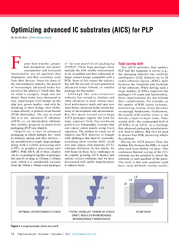
        are assembled in a single, large package   including  total  overlay  shift, yield   During the AICS process flow, the
        along with a central processing unit   loss and copper-clad laminate (CCL)   buildup film between the RDLs is cured
        (CPU) or graphics processing unit   substrate distortion. In this article, we   after each laser-drilled via layer. This
        (GPU). With AICS, all of these chiplets   will focus on these three challenges to   continuous thermal cycling of the CCL
        can be co-packaged together in packages   the rapidly growing AICS market and   substrate has the potential to distort the
        that may be as large as 120mm x 120mm   outline several solutions that we have   substrate in each quadrant of the panel.
        each, which is a considerable increase   determined will enable manufacturers   The result is that each quadrant could
        from the 10mm x 10mm-sized packages   to address them.                have vastly different overlay results.


        Figure 1: A visual explanation of total overlay drift.

        14
        14   Chip Scale Review   November  •  December  •  2023   [ChipScaleReview.com]

