Page 13 - Chip Scale Review_November-December_2023-digital
P. 13
Die placement accuracy
          Two bonding process cornerstones
        include bond force control and bond front
        propagation, of which the latter can be
        controlled through several options—with
        die shaping being preferred. The die shaping
        is responsible for creating a controlled
        bond front, ensuring no void entrapment,
        and avoiding ablation generated from the
        high-speed die bond to substrate wafer.
        Bond force, in turn, can impact initial bond
        strength from dielectric fusion as well as
        damage to the die if force is not controlled
        or not optimized.
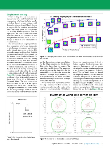
          Our approach to die shaping and bond
        front propagation is to have a single point
        of initial contact between die and substrate
        wafer, which is at the center of the die. This
        approach ensures two things: first, the initial
        contact causes instant bonding through Van
        der Waals’s forces, thereby locking the die   Figure 10: Die shaping height of die in µm vs. variation in the controllable factor for a 50µm (blue) and 100µm
        laterally and rotationally and minimizing   (red) thick die.
        placement accuracy loss from possible
        mechanical influences. Second, this allows   and that the maximum height is also higher.    The second scenario consists of direct, or
        the air between die and substrate wafer to   For the 100µm example, the die shows no   fusion, bonding. The first scenario uses
        be expelled symmetrically outwards as   deformation for the first four values of the   a process that does not rely on plasma
        the die is flattened, thereby ensuring equal   controlled-variable factor. The maximum   activation because the bonding mechanism
        conditions on all sides of the die as well   height is lower than the 50µm thick die, but   is not through instantaneous fusion by
        as minimizing risks of void entrapment.   both exhibit a similar behavior whereby the   way of Van der Waal’s forces, but through
        Figure 10 shows the shape of the same die   maximum die shape height flattens out. At   the temporary bonding material adhesive.
        at different values of the variable-controlled   all stages following the initial conditions   However, this process is reliant on the
        factor for a 7x7mm  die at thicknesses of   however, the first point of contact is always   TBM’s properties of bonding reaction times,
        50µm and 100µm. The inner orange circle   in the center of the die.   elasticity and viscosity among others, all of
        delineates that the die is at its highest   Two scenarios were explored to estimate   which have an impact on final accuracy. The
        warpage level taking on a convex shape.   bonding precision. The first scenario is   process was carried out with ~7x7mm dies
        The graph shows that for the thinner 50µm   bonding on a substrate wafer coated with a   analyzed using infrared (IR) microscopy.
        die, the change in shape occurs at a much   temporary bonding material (TBM) layer.   The results are shown in Figure 11 and
        lower value for the controlled variable factor


        Figure 9: Plot showing the effect of added queue
        time on bonding yield.             Figure 11: IR overlay for die placement on a wafer with a TBM layer.

                                                       Chip Scale Review   November  •  December  •  2023   [ChipScaleReview.com]  11 11

