Page 9 - Chip Scale Review_November-December_2023-digital
P. 9
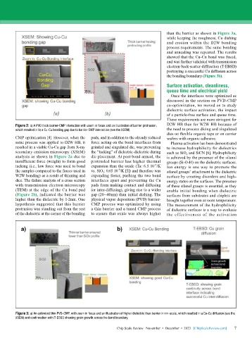
than the barrier as shown in Figure 3a,
                                                                              while keeping the roughness, Cu dishing
                                                                              and erosion within the D2W bonding
                                                                              process requirements. The same bonding
                                                                              and annealing was repeated. The results
                                                                              showed that the Cu-Cu bond was fused,
                                                                              and was further validated with transmission
                                                                              electron-back-scatter-diffraction (T-EBSD)
                                                                              portraying a successful Cu diffusion across
                                                                              the bonding boundary (Figure 3b).

                                                                              Surface activation, cleanliness,
                                                                              queue time and electrical yield
                                                                                Once the interfaces were optimized as
                                                                              discussed in the section on PVD-CMP
                                                                              co-optimization, we moved on to study
                                                                              dielectric surface activation, the impact
                                                                              of a particle-free surface and queue time.
                                                                              These requirements are more stringent for
        Figure 2: a) A PVD thick barrier-CMP interaction with zoom in focus and an illustration of barrier protrusion,   D2W HB than for W2W HB because of
        which resulted in b) a Cu-Cu bonding gap due to barrier-CMP interaction (see the XSEM).  the need to process dicing and singulated
                                                                              dies on flexible organic tape or on carrier
        CMP optimization [4]. However, when the   pads, and in addition to the already reduced   wafers with organic adhesive.
        same process was applied to D2W HB, it   force acting on the bond interfaces from   Plasma activation has been demonstrated
        resulted in a visible Cu-Cu gap from X-ray   grinded and singulated die, was preventing   to increase hydrophilicity for dielectrics
        secondary emission microscopy (XSEM)   the “tacking” of dielectric-dielectric during   such as SiO 2  and SiCN [6]. Hydrophilicity
        analysis as shown in Figure 2a due to   die placement. At post-bond anneal, the   is achieved by the presence of the silanol
        insufficient force (weight) to form good   protruded barrier has higher thermal   groups (Si-O-H) on the dielectric surfaces.
        tacking (i.e., low force was used to bond   expansion than the oxide (Ta: 6.5 10 /K   Ion energy is one way to promote the
                                                                         -6
        the samples compared to the forces used in   vs. SiO 2 : 0.65 10 /K [5]) and therefore was   silanol groups’ attachment to the dielectric
                                                        -6
        W2W bonding) as a result of thinning and   expanding faster, pushing the two bond   surface by creating disorders and high-
        dice. The failure analysis of a cross section   interfaces apart and preventing the Cu   energy states on the surfaces. The presence
        with transmission electron microscopy   pads from making contact and diffusing   of these silanol groups is essential, as they
        (TEM) at the edge of the Cu bond pad    (or inter-diffusing), giving rise to a wider   enable initial bonding when dielectric
        (Figure 2b), indicated the barrier was   gap (20~40nm) than initial dishing. The   surfaces from substrates and chiplets are
        higher than the dielectric by 1-2nm. One   physical vapor deposition (PVD) barrier-  brought together even at room temperature.
        hypothesis suggested that this barrier   CMP process was optimized by using   The measurement of the hydrophilicity
        protrusion was standing out from the rest   a thin barrier and a tuned CMP process   of dielectric surfaces is a way to evaluate
        of the dielectric at the corner of the bonding   to ensure that oxide was always higher   the effectiveness of the activation


        Figure 3: a) An optimized thin PVD-CMP, with zoom in focus and an illustration of higher dielectric than barrier in nm-scale, which resulted in a Cu-Cu diffusion (see the
        XSEM) and confirmation with T-EBSD showing grain growth across the bond boundary.

                                                       Chip Scale Review   November  •  December  •  2023   [ChipScaleReview.com]  7 7

