Page 8 - Chip Scale Review_November-December_2023-digital
P. 8
Die-to-wafer hybrid bonding development for HVM


        By Jonathan Abdilla  [BE Semiconductor Industries N. V.],  Guan Huei See  [Applied Materials, Inc.]


        T        his article addresses the key   back end of line (BEOL) inorganic dielectric   with the release of excessive water (H 2 O)


                 requirements for a successful
                                           issues noted above, as well as adding other
                 die-to-wafer (D2W) hybrid   and Cu, and is expected to improve over the   molecules, as well as metal-metal diffusion
                                                                              that will enable the electrical connection.
        bonding process. The selected process   benefits. Overall, the preparation needs for   A successful bond can be achieved
        steps from bonding pad formation to grind   die bonding are simplified, Cu bump and   with careful surface engineering of the
        and singulation, as well as an integrated   underfill processes are removed, and TCB   dielectric, typically with dielectric surface
        D2W bonding process will be addressed,   is replaced with room temperature HB. This   roughness values of <0.4nm [3]. Of the
        providing key technical values for the   directly translates into reduction of vertical   two HB flavors, wafer-to-wafer (W2W) or
        various steps involved. The integrated   form factor and scaling to higher input/  D2W, the latter enables higher system-level
        bonding processes include wet cleaning,   output (I/O) density, thereby leveraging the   yield thanks to use of known-good-dies
        degassing and plasma surface treatment.   mature BEOL that scaled well below the sub-  only. This paper describes the necessary
        Successful Cu-Cu diffusion through grain   micron range. The change of pad material   conditions to achieve a successful D2W HB
        growth across the boundary interface will   from a complex alloy (Cu-Ni-Sn-Ag) to pure   suitable for high-volume manufacturing
        show the efficacy of such a tool, C-mode   Cu and the direct connection through HB   (HVM) production.
        scanning acoustic microscopy (C-SAM)   at room temperature are expected to offer
        results will address the topic of voids, and   shorter interconnect lengths, lower resistance   PVD-CMP co-optimization
        electrical yield results will also be presented.   and improvement in thermal diffusion.   for D2W HB
        Actual placement accuracy results will also   As a result, an increase in system-level   As elegant as it looks, HB also has many
        be shared for both collective and direct D2W   performance with better bandwidth and/or   challenges. The bonding requirements
        hybrid bonding.                    speed can be expected.             that work for W2W HB, e.g., the Cu
                                             HB is achieved as a two-step process:   chemical mechanical polishing (CMP)
        Introduction                       first, by leveraging on the initial forces of   process that ensures good roughness
          The adoption of 3D architectures in   surface interaction at atomic proximity of   (<0.4nm), dishing (<5nm) and erosion,
        advanced packaging between chips is driven   the dielectric-dielectric interface to form   are not directly transferable to D2W. A
        by high-performance computing (HPC)   the “tacking,” which is the initiation of the   D2W test vehicle and bonding flow was
        and artificial intelligence (AI) requirements   bonding, and finally, following up with a   developed based on the illustration of the
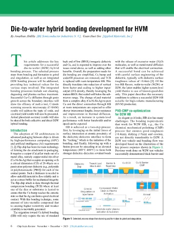
        [1, 2]. Flip chip has been the main technology   fusion process by annealing at an elevated   key process sequence shown in Figure 1.
        of forming the die attachment in packaging.   temperature (100°C-400°C) to form both   Previous work done on W2W test vehicles
        It requires a copper (Cu) pillar made out of a   stronger dielectric-dielectric covalent bonds   successfully demonstrated thick barrier and
        metal alloy, namely copper-nickel-tin-silver
        (Cu-Ni-Sn-Ag) that occupies an opening with
        a critical dimension (CD) of 20-40µm on a
        passivation polymer dielectric (e.g., polymide
        or polybenzoxazole [PBO]) for each of the
        contact points. Such a thickness is needed to
        allow underfill material to flow reliably and to
        act as a stress buffer for mechanical integrity.
        The flip-chip attach is done through thermal
        compression bonding (TCB) where at least
        one of the dies or substrates is heated to
        ensure that the Cu bump reaches the eutectic
        state so that Sn-Ag can form a good electrical
        contact. With this bonding technique, some
        amount of inter-metallic compound that
        is causing higher resistivity and weaker
        reliability is inevitably generated.
          The migration toward Cu hybrid bonding
        (HB) will only require the use of standard
                                           Figure 1: Selected process steps from bonding pad formation to grind and singulation.

        6 6  Chip Scale Review   November  •  December  •  2023   [ChipScaleReview.com]

