Page 10 - Chip Scale Review_November-December_2023-digital
P. 10
is free of organic residue and without
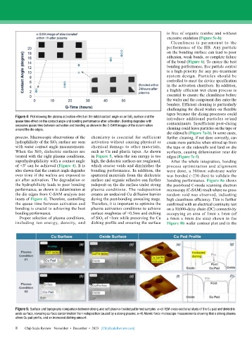
                                                                              excessive oxidation (Figure 5e-h).
                                                                                Cleanliness is paramount to the
                                                                              performance of the HB. Any particle
                                                                              on the bonding surface can lead to poor
                                                                              adhesion, weak bonds, or complete failure
                                                                              of the bond (Figure 6). To ensure the best
                                                                              bonding performance, free particle control
                                                                              is a high priority for any pre-treatment
                                                                              system design. Particles should be
                                                                              controlled to meet the device specification
                                                                              in the activation chambers. In addition,
                                                                              a highly efficient wet clean process is
                                                                              essential to ensure the cleanliness before
                                                                              the wafer and the component dies enter the
                                                                              bonders. Efficient cleaning is particularly
                                                                              challenging for diced wafers on flexible
                                                                              tapes because the dicing processes could
        Figure 4: Plot showing the plasma activation effect on the initial contact angle on an SiO 2  surface and the   introduce additional particles or/and
        queue time effect on the contact angle and bonding performance after activation. Bonding degrades with   contaminants. Insufficient post-dicing
        excessive queue time between activation and bonding as shown in the C-SAM images of the delamination
        around the die edges.                                                 cleaning could leave particles on the tape or
                                                                              die sidewalls (Figure 7a-b). In some cases,
        process. Macroscopic observations of the   chemistry is essential for sufficient   further cleaning, if not done correctly, can
        hydrophilicity of the SiO 2  surface are seen   activation without causing physical or   create more particles when stirred up from
        with water contact angle measurements.   chemical damage to other materials,   the tape or die sidewalls and land on die
        When the SiO 2  dielectric surfaces are   such as Cu and plastic tapes. As shown   surfaces, causing delamination near die
        treated with the right plasma conditions,   in Figure 5, when the ion energy is too   edges (Figure 7c-f).
        superhydrophilicity with a contact angle   high, the dielectric surfaces are roughened,   After the whole integration, bonding
        of <5º can be achieved (Figure 4). It is   which creates voids and diminishes the   process optimization and alignment
        also shown that the contact angle degrades   bonding performance. In addition, the   were done, a 300mm substrate wafer
        over time if the wafers are exposed to   sputtered materials from the dielectric   was bonded (~230 dies) to validate the
        air after activation. The degradation or   surface and organic adhesive can further   bonding performance. Figure 8a shows
        the hydrophilicity leads to poor bonding   redeposit on the die surface under strong   the post-bond C-mode scanning electron
        performance, as shown in delamination at   plasma conditions. The redeposition   microscopy (C-SAM) result where no gross
        the die edges from C-SAM analysis (see   creates an undesired Cu diffusion barrier   random void was observed, indicating
        insets of Figure 4). Therefore, controlling   during the post-bonding annealing stage.   high cleanliness efficiency. This is further
        the queue time between activation and   Therefore, it is important to optimize the   confirmed with an electrical continuity test
        bonding is crucial to achieving the best   plasma activation conditions to achieve   on a 10,000-daisy chain (DC) connectivity
        bonding performance.               surface roughness of <0.5nm and etching   occupying an area of 1mm x 1mm (of
          Proper selection of plasma conditions,   of SiO 2  of <1nm while preserving the Cu   a 6mm x 6mm die size) shown in the
        including ion energy, density, and   dishing profile and ensuring the surface   Figure 8b wafer contour plot and in the


        Figure 5: Surface and topography comparison between strong and soft plasma-treated patterned samples: a–d) TEM cross-sectional study of the Cu pad and dielectric
        oxide surface, revealing surface contamination from redeposition caused by a strong plasma; e–h) Atomic force microscope measurements showing that a strong plasma
        alters Cu pad profile, and an increased dishing amount.

        8 8  Chip Scale Review   November  •  December  •  2023   [ChipScaleReview.com]

