Page 15 - Chip Scale Review_November-December_2023-digital
P. 15
The importance of cleanliness was clearly
                                                                              stated and demonstrated via studies
                                                                              showing void formations arising from
                                                                              particle entrapment. The bonding process
                                                                              itself was accomplished with advanced
                                                                              dynamic die-shaping capabilities, state of
                                                                              the art alignment (162nm @ 3σ), and using
                                                                              inline control capability. Finally, control of
                                                                              the queue time along the whole process is
                                                                              critical to guarantee optimal yield.

                                                                              Acknowledgments
                                                                                Portions of this article were presented
                                                                              at the IMAPS Device Conference 2023.
                                                                              Additional co-authors are: Ying Wang,
                                                                              Raymond Hung, Yauloong RuiPing
                                                                              Wang, Arvind Sundarrajan of Applied
                                                                              Materials, Inc., Hybrid Bonding Centre of
                                                                              Excellence; and Stefan Schmid, Benedikt
                                                                              Auer, Djuro Bikaljevic, PC Koay,
                                                                              Nithyananda Hegde, and Chris Scanlan of
                                                                              BE Semiconductor Industries N.V.

                                                                              References
                                                                                 1.  W. L. I. C. C. a. C. H. Chiu, “Low-
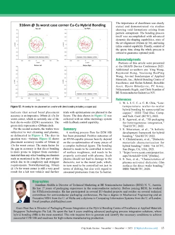
        Figure 12: IR overlay for die placement on a wafer with direct bonding including a copper pad.  temper at u re wafer-to -wafer
                                                                                   hybrid bonding by nanocrystalline
        indicate that actual bond placement   trials with optimizations are planned in the   copper,”  IEEE 72nd Elec. Comp.
        accuracy is an impressive 160nm @ ±3s for   future. The data shown in Figure 12 was   and Tech. Conf. (ECTC), 2022.
        worst corner, which is currently one of the   collected with an inline metrology system   2.  R. Agarwal, et al., “3D packaging
        best die-to-wafer (D2W) accuracies. The   with feedback control capability.   for heterogeneous integration,”
        green circle represents a ±200nm circle.                                   72nd ECTC, 2022.
          For the second scenario, the wafers were   Summary                     3.  S. Sitaraman, et al., ”A holistic
        subjected to wet cleaning and plasma,   A working process flow for D2W HB   development framework for hybrid
        as delineated in Figure 1. The dies in   has been presented. Positive outcomes of   bonding,” 72nd ECTC 2022.
        question were ~6x6mm. Figure 12 shows   an HVM-capable process heavily depend   4.  V. Chidambaram, et al., ”Dielectric
        placement accuracy results of 316nm @   on the co-optimization of many pieces of   materials characterization for
        ±3s for worst corner. The main factor for   a complex technical jigsaw. The bonding   hybrid bonding,” IEEE 71st ECTC,
        the gap in accuracy is that direct bonding   dielectric needs to be controlled in terms   San Diego, CA, USA, 2021.
        is more prone to impact from customer   of surface roughness, and needs to be   5.  “https://www.azom.com/properties.
        material than any other bonding mechanism   properly activated with plasma. Such   aspx?ArticleID=1114,” [Online].
        such as mentioned in the first part of this   plasma should not lead to damage to the   6.  S. Son, et al., “Characteristics of
        article due to its complexity and stringent   dielectric, nor to the metal pads, which,   plasma-activated dielectric film
        requirements. Notwithstanding, 316nm   in turn need to be controlled not just in   surfaces for direct wafer bonding,”
        @ ±3s for worst corner is still a very good   terms of dishing, but also with regard to   IEEE 70th ECTC, 2020.
        result for a lab test vehicle and further   unwanted protrusions from the Ta barrier.


                       Biographies
                         Jonathan Abdilla is Director of Technical Marketing at BE Semiconductor Industries (BESI) N. V., Austria.
                       He has 17 years of packaging experience in the semiconductor industry. Before joining BESI, he worked
                       for STMicroelectronics. He has participated in several EU-funded projects and resides on several technical
                       committees for semiconductor packaging conferences. He has a degree in Mechanical Engineering and an
                       Executive MBA from the U. of Malta and a diploma in Computing Information Systems from the U. of London.
                       Email jonathan.abdilla@besi.com

            Guan Huei See is Director of Packaging Process Integration at the Hybrid Bonding Centre of Excellence at Applied Materials
          Singapore Technologies Pte Ltd. He spent the last 8 years enabling advanced packaging process integration solutions, where
          hybrid bonding (HB) is the most essential. This role requires him to generate and identify the necessary conditions to achieve
          successful C2W HB and readiness for high-volume manufacturing production.


                                                                                                             13
                                                       Chip Scale Review   November  •  December  •  2023   [ChipScaleReview.com]  13

