Page 46 - Chip Scale Review_September-October_2023-digital
P. 46
overall thermal resistance in advanced   properties of the materials at different   the Boltzmann transport equation (BTE)
        packages. The introduction of backside   dimensional scales and levels of detail.   (Figure 1b). The model additionally
        power delivery schemes (moving the   Each model can be used by itself,   captures thermal effects at the nanoscale.
        entire power distribution network   depending on the use case of interest.   The material properties of metals
        to the chip’s backside) and novel   The output of each of the models can   and  dielectrics,  as  characterized  on
        transistor architectures (such as gate-  also be used as input for the next,   dedicated test structures, are used
        all-around nanosheets) in the logic   enabling a complete analysis of a full   as an input for the model. For the
        roadmap may impact the temperature   BEOL stack. The modeling work is   dielectrics, for example, the so-called
        of the metal lines as well—in a good   combined with experimental data   3ω method was used to experimentally
        or bad sense.                      obtained on test vehicles with industry-  ext ract the ther mal conductivit y
          A more comprehensive modeling    relevant materials and dimensions. The   of r eleva nt d iele ct r ic m at e r ia l s
        framework is needed to capture the   measured data are fed into the models,   very precisely, revealing a value of
        impact of these innovations on heat   allowing for accurate calibration and   1.15W/mK for SiO 2  and 0.3W/mK for
        propagat ion a nd to en ha nce ou r   prediction of future scenarios.  OSG3.0 (an organosilicate glass with 3.0
        fundamental  understanding of how                                     dielectric constant).
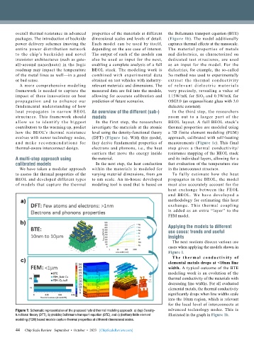
        heat propagates in nar row BEOL    An overview of the different (sub-)  In the third step, the researchers
        structures. This framework should   models                            zoom out to a larger par t of the
        allow us to ident if y t he biggest   In  the  first  step,  the  researchers   BEOL layout. A full BEOL stack’s
        contributors to the warming up, predict   investigate the materials at the atomic   thermal properties are modeled using
        how  the BEOL’s  thermal resistance   level using the density-functional theory   a 3D finite element modeling (FEM)
        evolves with newer technology nodes,   (DFT) (Figure 1a). With this model,   approach, calibrated with self-heating
        a nd m a ke r e c om me nd at ion s for   they derive fundamental properties of   measurements (Figure 1c). This final
        thermal-aware interconnect design.  electrons and phonons, i.e., the heat   step gives a thermal conductivity/
                                           carriers that move the energy inside    resistance mapping of the BEOL stack
        A multi-step approach using        the material.                      and its individual layers, allowing for a
        calibrated models                    In the next step, the heat conduction   fast evaluation of the temperature rise
          We have taken a modular approach   within the materials is modeled for   in the interconnect structure.
        to assess the thermal properties of the   varying material dimensions, from µm   To f ully estimate how the heat
        BEOL and developed different types   to nm scale. An in-house developed   propagates  in  the  BEOL,  the  model
        of models that capture the thermal   modeling tool is used that is based on   must also accurately account for the
                                                                              heat exchange between the FEOL
                                                                              and BEOL. We have developed a
                                                                              methodology for estimating this heat
                                                                              exchange. This ther mal coupling
                                                                              is added as an extra “layer” to the
                                                                              FEM model.

                                                                              Applying the models to different
                                                                              use cases: trends and useful
                                                                              insights
                                                                                The next sections discuss various use
                                                                              cases when applying the models shown in
                                                                              Figure 1.
                                                                                T he ther ma l conduc t i v it y of
                                                                              elemental metals drops at <10nm line
                                                                              width. A typical outcome of the BTE
                                                                              modeling work is an evolution of the
                                                                              thermal conductivity of the materials with
                                                                              decreasing line widths. For all evaluated
                                                                              elemental metals, the thermal conductivity
                                                                              significantly drops when line widths scale
                                                                              into the 10nm region, which is relevant
                                                                              for the local level of interconnects at
        Figure 1: Schematic representation of the proposed hybrid thermal modeling approach: a) (top) Density-  advanced technology nodes. This is
        functional theory (DFT), b) (middle) Boltzmann transport equation (BTE), and c) (bottom) finite element   illustrated in the graph in Figure 1b.
        modeling (FEM) based models capture thermal properties at different dimensional scales.

        44
        44   Chip Scale Review   September  •  October  •  2023   [ChipScaleReview.com]

