Page 43 - Chip Scale Review_September-October_2023-digital
P. 43
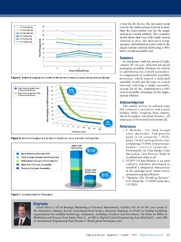
a four-die HI device, the increased scrap
                                                                              cost for the multi-system solution is more
                                                                              than the depreciation cost for the single
                                                                              system per circuit solution. The economic
                                                                              model shows that even if the multi-system
                                                                              solution is free, the increased scrap,
                                                                              operator, and utilization costs result in the
                                                                              single-system solution delivering a 60%
                                                                              lower overall assembly cost.
                                                                              Summary
                                                                                In conclusion, with the advent of high-
                                                                              volume HI circuits, efficient advanced
                                                                              packaging assembly solutions are critical
                                                                              to optimizing the overall economics.
                                                                              A comparison of traditional assembly
        Figure 5: Relative throughput as a function of the number of unique die types and quantity per die type.  processes, which require a dedicated
                                                                              assembly system per die type, to a novel
                                                                              solution utilizing a single-assembly
                                                                              system for all die, demonstrates a 60%
                                                                              cost of assembly advantage for the single-
                                                                              system solution.
                                                                              Acknowledgment
                                                                                The author wishes to acknowledge
                                                                              the solution’s  inventors and patent
                                                                              holders: Mike Yingling, Sean Adams,
                                                                              David Lyndaker, and Scott Proctor—all
                                                                              employees of Universal Instruments [3].
                                                                              References
                                                                                1.  J. H r u s k a , “A s c h i p d e sig n
                                                                                  costs skyrocket, 3nm process
                                                                                  no de i s i n je op a rdy,” 2020;
        Figure 6: Relative throughput as a function of circuits per carrier and wafer exchange time.
                                                                                  https://www.extremetech.com/
                                                                                  computing/272096-3nm-process-
                                                                                  n o d e # :~: t e x t = i n Je o p a r d y |
                                                                                  Extremetech-,As Chip Design Costs
                                                                                  Skyrocket, 3nm Process Node Is
                                                                                  in,afford new chips at all.
                                                                                2.  UCIe™ 1.0 Specification is an open
                                                                                  industry standard developed to
                                                                                  establish a ubiquitous interconnect
                                                                                  at the package level; https://www.
                                                                                  uciexpress.org/specification
                                                                                3.  “Modular Die Handling System,”
                                                                                  U.S. Patent No. 11164765 Issue date:
                                                                                  11/2/2021.


        Figure 7: Economic model for HI assembly.


                       Biography
                         Glenn Farris is VP of Strategic Marketing at Universal Instruments, Conklin, NY. In his 30+ year career in
                       the electronics industry, he has transitioned from being a Research Engineer at NASA to leading marketing
                       organizations for multiple technology companies, including Teradyne and Formfactor. He holds an MBA in
                       Marketing and Finance from Santa Clara U., an MS in Digital Control Engineering from Stanford U., and a BS
                       in Aeronautical Engineering from Purdue U. Email glenn.farris@uic.com.


                                                                                                             41
                                                         Chip Scale Review   September  •  October  •  2023   [ChipScaleReview.com]  41

