Page 39 - Chip Scale Review_September-October_2023-digital
P. 39
Efficiency and cost implications of multi-die


        heterogeneous integration


        By Glenn Farris  [Universal Instruments]
        T        he semiconductor industry is actively working


                 towards achieving widespread integration  of
                 diverse semiconductor die types through a
        technique known as heterogeneous integration (HI). These die
        can originate from various wafer sizes and are produced using
        different technological processes. This emerging packaging
        method presents fresh challenges related to the efficiency of
        assembly and the overall yield.
          Historically, the process of flip-chip assembly has employed
        a single tool to position a singular die type onto the intended
        substrate. In cases involving multiple die types, manufacturing
        lines have been configured with a sequence of placement
        tools, each designated for a specific die type. This article
        delves into the implications of such an approach in the context
        of the  HI era. The effects on product yield, production
        speed, manufacturing efficiency, and the comprehensive
        cost of assembly are investigated across a wide array of HI
        die setups.
          An innovative strategy is proposed for optimizing the
        comprehensive economic aspects of the assembly. This
        strategy is based on a sensitivity analysis encompassing the   Figure 1: Design cost by node.
        expected range of die types applicable in these scenarios.   a single tool. A sensitivity analysis for a broad range of die
        The viability of this new approach is examined for various   configurations can be assessed by modeling the impact on the
        packaging solutions, including flip-chip, 2.5D, 3D, and fan-  five major cost categories for multiple dedicated placement tools
        out technologies.                                    versus a single-tool solution.
        Introduction                                         HI circuit characteristics
          While transistor scaling continues, the economic     The following sections discuss various HI circuit
        improvements derived from this scaling, typically referred to   characteristics.
        as Moore’s Law, have been diminishing. For example, over   Device types and quantity per substrate. The number of
        the past decade, at nodes below 22nm, the associated costs to   devices per HI circuit ranges from a minimum of two device
        design and introduce new products have increased by a factor   types and may be as high as 8 unique devices. These die
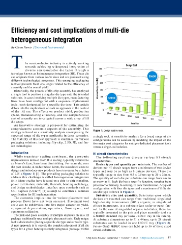
        of 7.75. (Figure 1) [1]. The prevailing packaging solution to   typically range in size from 0.5 x 0.5mm up to 20 x 20mm.
        address this challenge is called heterogeneous integration   The quantity of each die per substrate can range from one to
        (HI). Many studies have focused on a chip-to-chip signaling,   as many as 8. Each die has a specific function, ranging from
        power distribution, materials, thermals, bonding metallurgy,   processor to memory, to sensing, to data transmission. A typical
        and design methodologies. Interface open standards such as   configuration with four die types and a maximum of 8 die for
        UCI Express (UCIe™) [2] attempt to establish a common   one die type is shown in Figure 2.
        specification for HI implementation.                   Substrate size and quantity. Substrates upon which
          The economic implications for various placement tool   devices are mounted can range from traditional singulated
        process f lows have not been assessed. Placement tool   high-density interconnect (HDI) organic, to singulated
        costs can be subdivided into five major categories: yield,   silicon interposers, to a substrate-less wafer or panel fan-
        equipment depreciation, operators, f loor space, and   out. In the case of singulated organic substrates, these are
        equipment utilization.                               typically presented to the pick and place assembly tool via
          The pick-and-place assembly of multiple disparate die in a HI   a JEDEC standard tray (or Gen2 JEDEC tray in the future).
        package traditionally uses multiple placement tools. Each unique   At substrate dimensions up to 31 x 44mm, up to 28 circuit
        tool is dedicated to placing a specific die type and/or wafer type.   substrates can be loaded in one JEDEC tray (Figure 3).
        A new approach is to execute the complete placement of all die   Future Gen2 JEDEC trays can hold up to 56 of these sized
        types for a given heterogeneously-integrated package within   circuit substrates.

                                                                                                             37
                                                         Chip Scale Review   September  •  October  •  2023   [ChipScaleReview.com]  37

