Page 40 - Chip Scale Review_September-October_2023-digital
P. 40
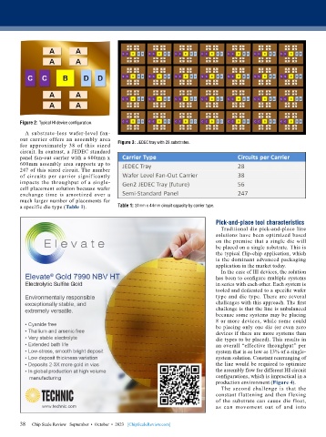
Figure 2: Typical HI device configuration.
          A substrate-less wafer-level fan-
        out  carrier  offers  an  assembly  area
        for approximately 38 of this sized   Figure 3: JEDEC tray with 28 substrates.
        circuit. In contrast, a JEDEC standard
        panel fan-out carrier with a 600mm x
        600mm assembly area supports up to
        247 of this sized circuit. The number
        of circuits per carrier significantly
        impacts the throughput of a single-
        cell placement solution because wafer
        exchange time is amortized over a
        much larger number of placements for
        a specific die type (Table 1).     Table 1: 31mm x 44mm circuit capacity by carrier type.

                                                                              Pick-and-place tool characteristics
                                                                                Traditional die pick-and-place line
                                                                              solutions have been optimized based
                                                                              on the premise that a single die will
                                                                              be placed on a single substrate. This is
                                                                              the typical flip-chip application, which
                                                                              is the dominant advanced packaging
                                                                              application in the market today.
                                                                                In the case of HI devices, the solution
                                                                              has been to configure multiple systems
                                                                              in series with each other. Each system is
                                                                              tooled and dedicated to a specific wafer
                                                                              type and die type. There are several
                                                                              challenges with this approach. The first
                                                                              challenge is that the line is unbalanced
                                                                              because some systems may be placing
                                                                              8 or more devices, while some could
                                                                              be placing only one die (or even zero
                                                                              devices if there are more systems than
                                                                              die types to be placed). This results in
                                                                              an overall “effective throughput” per
                                                                              system that is as low as 13% of a single-
                                                                              system solution. Constant rearranging of
                                                                              the line would be required to optimize
                                                                              the assembly flow for different HI circuit
                                                                              configurations, which is impractical in a
                                                                              production environment (Figure 4).
                                                                                The second challenge is that the
                                                                              constant flattening and then flexing
                                                                              of the substrate can cause die float,
                                                                              as  can  movement  out  of  and  into


        38   Chip Scale Review   September  •  October  •  2023   [ChipScaleReview.com]
        38

