Page 51 - Chip Scale Review Sep Oct_2022-digital
P. 51

for 1,000 hours at 175°C to stress
                                                                              the braze metal and prove that the
                                                                              brazing filler metal system is stable.
                                                                              No difference was observed between
                                                                              t h e  i n i t i a l  s t a t u s a n d t h e  a g e d
                                                                              substrate after HTS, showing that the
                                                                              alloy system displays no degradation
                                                                              and consistent values after 1,000
                                                                              hours of aging at 175°C.
                                                                              Thermal resistance simulation
                                                                                A t h e r m a l s i m u l a t i o n w a s
                                                                              performed to assess the inf luence
                                                                              of t her mal conduct ivit y a nd t he
                                                                              thickness of the braze metal layers in
                                                                              the substrate on its total thermal re-
                                                                              sistance. To include heat spreading
                                                                              and other geomet r ical effects, a
                                                                              finite element method (FEM) was
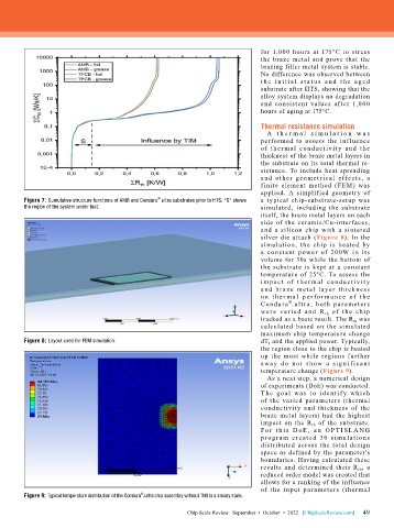
                                                                              applied. A simplified geometry of
                                                ®
        Figure 7: Cumulative structure functions of AMB and Condura .ultra substrates prior to HTS. “S” shows   a typical chip-substrate-setup was
        the region of the system under test.                                  simulated, including the substrate
                                                                              itself, the braze metal layers on each
                                                                              side of the ceramic/Cu-interfaces,
                                                                              and a silicon chip with a sintered
                                                                              silver die attach (Figure 8). In the
                                                                              simulation, the chip is heated by
                                                                              a  constant  power  of  200W  in  its
                                                                              volume  for  30s  while  the  bottom  of
                                                                              the substrate is kept at a constant
                                                                              temperature of 25°C. To assess the
                                                                              i mp a c t of t he r m a l c ond uc t iv it y
                                                                              a nd bra ze met al layer t h ick ness
                                                                              o n t h e r m a l p e r fo r m a n c e of t h e
                                                                              Condu ra .ult ra, both parameters
                                                                                       ®
                                                                              we re va r ie d a nd R th  of t he ch ip
                                                                              tracked as a basic result. The R th  was
                                                                              calculated based on the simulated
                                                                              maximum chip temperature change
        Figure 8: Layout used for FEM simulation.                             dT J  and the applied power. Typically,
                                                                              the region close to the chip is heated
                                                                              up the most while regions further
                                                                              away do not show a sig n i f ica nt
                                                                              temperature change (Figure 9).
                                                                                As a next step, a numerical design
                                                                              of experiments (DoE) was conducted.
                                                                              T he goal wa s t o ide nt if y wh ich
                                                                              of the varied parameters (thermal
                                                                              conductivity and thickness of the
                                                                              braze metal layers) had the highest
                                                                              impact on the R th  of the substrate.
                                                                              Fo r t h i s D o E , a n  O P T IS L A N G
                                                                              prog r a m created 30 si mu lat ion s
                                                                              distributed across the total design
                                                                              space as defined by the parameter’s
                                                                              boundaries. Having calculated these
                                                                              results and determined their R th , a
                                                                              reduced order model was created that
                                                                              allows for a ranking of the influence
                                                                              of the input parameters (ther mal
                                           ®
        Figure 9: Typical temperature distribution of the Condura .ultra chip assembly without TIM in a steady state.
                                                                                                             49
                                                         Chip Scale Review   September  •  October  •  2022   [ChipScaleReview.com]  49
   46   47   48   49   50   51   52   53   54   55   56