Page 48 - Chip Scale Review Sep Oct_2022-digital
P. 48
with the die on the substrate. This
                                                                              way, thick copper wires or ribbons
                                                                              c a n b e w e d g e b o n d e d w i t h ou t
                                                                              breaking the  die  (Figure 2b).  The
                                                                              benefits of copper wire bonding and
                                                                              DTS  are discussed in the second
                                                                                   ®
                                                                              part of the article.
                                                                              Phase formation
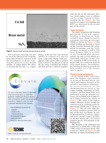
                                                                                The phase formation and bonding
                                                                              m e c h a n i s m of ou r n e w c o p p e r-
                                                                              b o n d i n g t e c h no l o g y  o n  S i 3 N 4
                                                                              cer a m ics were cha r acter i zed by
                                                                              s ca n n i n g  e l e c t r o n  m i c r osc o p y
                                                                              (SEM) as shown in  Figure 3. The
                                                                              actual bonding mechanism is based
                                                                              on the reaction between the active
                                                                              m e t a l (t i t a n i u m) a n d t h e Si 3 N 4
                                                                              c e r a m i c , fo r m i ng a s t a bl e Ti N
        Figure 3: Typical Condura .ultra microstructure measured by SEM.
                         ®
                                                                              layer. Because there is no silver
          Silver pressure sintering can also   plates, with ou r Die Top System   i n t h e C o n d u r a ®.u l t r a s y s t e m ,
                                                 ®
        be used for advanced die frontside   ( DTS ).  It  consists  of  a  thi n  Cu   typical Ag- and Cu-rich phases are
        interconnections as reported with   plate (t y pically 50µm) with pre-  eliminated, which are known from
        t h e a t t a c h m e n t of m e t a l cl i p s ,   applied sinter paste, that is picked   the standard AMB technology as
        f le x i ble  p r i n t e d c i r c u it  b o a r d s   from a carrier to be placed on top of   using high Ag-containing brazing
        (PCBs), or copper plates. We chose   the die using a standard die bonder   f iller metal pastes. Nevertheless,
        to develop the  last  one, i.e., copper   and then pressure-sintered together   the bonding mechanism towards the
                                                                              Si 3 N 4   ceramic  via a TiN reaction
                                                                              layer is similar.

                                                                              Thermal shock performance
                                                                                S i 3 N 4 - b a s e d A M B s u b s t r a t e s
                                                                              m e e t  t h e h i g h e s t  r e q u i r e m e n t s
                                                                              i n t e r m s of t h e r m a l  sho c k t e s t
                                                                              (TST) performance because of the
                                                                              ceramic’s mechanical robustness.
                                                                              To a s s e s s r e s i s t a n c e v s . t h e
                                                                              t he r mome cha n ical st re ss of ou r
                                                                              copper bonding technology on Si 3 N 4
          For over a decade, Technic’s Elevate                                ceramics, thermal shock tests were
                                        ®
          Chemistry has risen to meet the                                     perfor med using an inter nal test
                                                                                                2
          greatest challenges of our industry                                 layout (30.6x29mm  with 0.5mm Cu
          with innovation, expertise, exceptional                             on 0.32mm ceramic) as shown in
          analytical support, and the best                                    Figure 4. The status of the copper-
          customer service in the industry.                                   bonded substrates before testing was
                                                                              characterized by scanning acous-tic
                                                                              microscopy (SAM) and is shown in
            •  Electroplating Solutions for                                   Figure 4a. The red color indicates
                 Copper                                                       an etched isolation groove that is
                 Nickel & Tin                                                 part of the used test layout. In case
                 Precious Metals                                              of delam i nat ion bet ween copper
            •  Photoresist Strippers                                          and braze metal/ceramic because
            •  Metal Etchants                                                 of thermal shock, the red-colored
            •  Post Etch Residue Removers                                     isolation groove will broaden in the
                                                                              SAM picture.
                                                                                The integrity of the substrates was
                                                                              reassessed by SAM after 3,000 and
                                                                              5,000 cycles of thermal shock. The
                                                                              results are shown in  Figure 4b and
                                                                              illustrate no major broadening of the
          Learn more at www.technic.com

                                                             1/19/2022   10:41:44 AM
          Chip Scale Review - Jan-Feb 2022.indd   1          1/19/2022   10:41:44 AM
          Chip Scale Review - Jan-Feb 2022.indd   1
        46   Chip Scale Review   September  •  October  •  2022   [ChipScaleReview.com]
        46

