Page 50 - Chip Scale Review Sep Oct_2022-digital
P. 50

failure mode is also often observed
                                                                              for Ag-containing AMB substrates.
                                                                              However, there is no failure within
                                                                              the reaction zone of the substrate
                                                                              with the copper-bonded technology.
                                                                              This is proven by energy dispersive
                                                                              spectroscopy (EDS) phase mapping
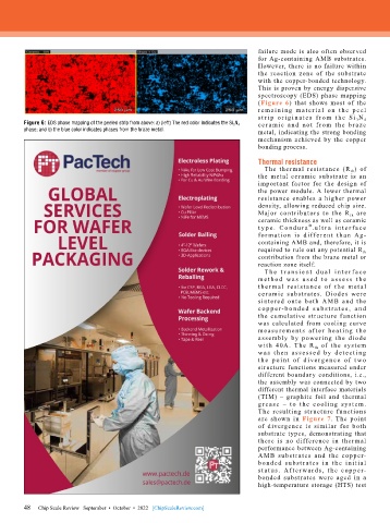
                                                                              (Figure  6)  that  shows  most  of  the
                                                                              r e m a i n i ng m at e r ia l on t he p e el
                                                                              s t r ip o r ig i n a t e s f r o m t h e Si 3 N 4
        Figure 6: EDS phase mapping of the peeled strip from above: a) (left) The red color indicates the Si 3 N 4    cer a m ic a nd not f rom t he br a ze
        phase; and b) the blue color indicates phases from the braze metal.   metal, indicating the strong bonding
                                                                              mechanism achieved by the copper
                                                                              bonding process.
                                                                              Thermal resistance
                                                                                The ther mal resistance (R th ) of
                                                                              the metal ceramic substrate is an
                                                                              important factor for the design of
                                                                              the  power  module.  A  lower  thermal
                                                                              resistance enables a higher power
                                                                              density, allowing reduced chip size.
                                                                              Major contributors to the R th  are
                                                                              ceramic thickness as well as ceramic
                                                                              t y p e .  C o n d u r a .u l t r a  i n t er f ac e
                                                                                              ®
                                                                              for m at ion is d if fe re nt t ha n Ag-
                                                                              containing AMB and, therefore, it is
                                                                              required to rule out any potential R th
                                                                              contribution from the braze metal or
                                                                              reaction zone itself.
                                                                                T h e t r a n s i e n t d u a l i n t e r f a c e
                                                                              m e t ho d wa s u s e d t o a s s e s s t h e
                                                                              t he r m al re sist a nce of t he met al
                                                                              ceramic subst rates. Diodes  were
                                                                              sintered  onto  both  A MB  and  the
                                                                              co p p e r- bo n d e d  su b s t r a t e s,  a n d
                                                                              the cumulative structure function
                                                                              was calculated from cooling curve
                                                                              me a su re me nt s  af t e r  he at i ng  t he
                                                                              assembly by power ing the diode
                                                                              with  40A. T he  R th  of the system
                                                                              wa s  t he n  a s se s se d  by  det e c t i ng
                                                                              t h e p oi n t of d ive r ge n c e of t wo
                                                                              structure functions measured under
                                                                              different boundary conditions, i.e.,
                                                                              the assembly was connected by two
                                                                              different thermal interface materials
                                                                              (TIM) – graphite foil and thermal
                                                                              g rea se – to t he cool i ng system.
                                                                              The resulting structure functions
                                                                              are  shown  in  Figure  7.  The  point
                                                                              of divergence is similar for both
                                                                              substrate types, demonstrating that
                                                                              there is no difference in ther mal
                                                                              performance between Ag-containing
                                                                              A MB subst rates and the copper-
                                                                              bonded subst r ates i n t he i n it ial
                                                                              st at u s. A f t e r wa rd s,  t he copp e r-
                                                                              bonded  substrates were aged in a
                                                                              high-temperature storage (HTS) test


        48   Chip Scale Review   September  •  October  •  2022   [ChipScaleReview.com]
        48
   45   46   47   48   49   50   51   52   53   54   55