Page 47 - Chip Scale Review Sep Oct_2022-digital
P. 47
Silver-free AMB and copper bonding for cost-efficient,


        reliable advanced packaging


        By A. Schwöbel, C. Féry, B. Fabian, D. Schnee, M. Rauer, A. Miric, S. Gunst  [Heraeus Deutschland GmbH & Co. KG]
        H          igh-power electronics have   are the major price drivers for AMB   conducted. Results of the experiments


                   become one of the fastest
                                                                                R e g a r d i n g t h e a t t a c h m e n t of
                                           design-to-cost, highly-reliable Ag-
                   growing market segments   subst rates. We have developed a   follow in the first part of this article.
        of the semiconductor industry. Major   f r e e t h ick-f i l m c o p p e r b ond i ng   dies to metal ceramic substrates,
                                                     ®
        applications  include  motor  drives,   (Condu r a .u lt r a) t e ch nolog y for   a clear trend is the replacement of
        hybrid/electric vehicles, rail traction,   joining nitride-based ceramics with   conventional soldering with silver
        w i nd  t u rbi nes,  a nd  photovolt aic   Cu foils. The paste eliminates the   pressure sintering when higher power
        inverters. Because the power electronic   use of an expensive vacuum-based   densities are required. With a melting
        modules used in these applications   brazing technology. But how does   temperat ure of 961°C, a sintered
        operate at high voltage and high   this new bonding technology perform   silver bonding layer enables operating
        current density, they must handle high   compared to the industry-benchmark   temperatures above 200°C, whereas a
        temperatures and harsh conditions.   A M B subst rate? To compare the   lead-free soldered joint, with a melting
        One of the key components for highly   performance between the two kinds   temperature of about 230°C, quickly
        reliable power electronic modules is   of substrates, various re-liability-   deg rades. Fu r ther more, the heat
        a reliable metal ceramic substrate. To   and  application-related  tests  such   transport through the joining layer is
        provide reliable functionality during   as thermal shock (-65°C/+150°C),   significantly better with Ag sintering
        operation, the substrate materials   peel strength, and high-temperature   rather than with soldering (>200W/m/
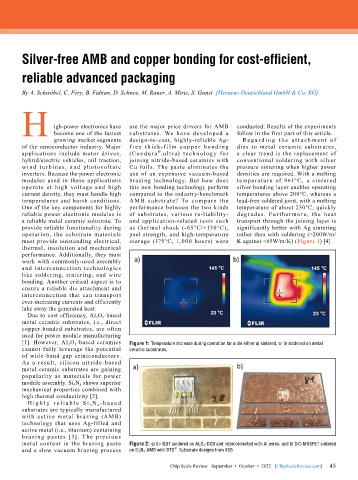
        must provide outstanding electrical,   storage (175°C, 1,000 hours) were   K against <65W/m/K) (Figure 1) [4].
        thermal, insulation and mechanical
        performance. Additionally, they must
        work with commonly-used assembly
        and  interconnection  technologies
        like soldering, sintering, and wire
        bonding. Another critical aspect is to
        ensure a reliable die attachment and
        interconnection that can transport
        ever-increasing currents and efficiently
        take away the generated heat.
          Due to cost efficiency, Al 2 O 3 -based
        metal ceramic substrates, i.e., direct
        copper-bonded substrates, are often
        used for power module manufacturing
        [1]. However, Al 2 O 3 -based ceramics   Figure 1: Temperature increase during operation for a die either a) sintered, or b) soldered on metal
        cannot fully leverage the potential   ceramic substrates.
        of wide-band-gap semiconductors.
        As a result, silicon nitride-based
        metal ceramic substrates are gaining
        popularity  as  materials  for  power
        module assembly. Si 3 N 4  shows superior
        mechanical properties combined with
        high thermal conductivity [2].
          H i g h ly  r e l i a b l e  S i 3 N 4 - b a s e d
        substrates are typically manufactured
        with active metal brazing (AMB)
        technology that uses Ag-filled and
        active metal (i.e., titanium) containing
        brazing pastes [3]. The precious
        metal content in the brazing paste   Figure 2: a) Si-IGBT soldered on Al 2 O 3 -DCB and interconnected with Al wires; and b) SiC-MOSFET sintered
                                                          ®
        and a slow vacuum brazing process   on Si 3 N 4 -AMB with DTS . Substrate designs from IISB.
                                                                                                             45
                                                         Chip Scale Review   September  •  October  •  2022   [ChipScaleReview.com]  45

