Page 53 - Chip Scale Review Sep Oct_2022-digital
P. 53
with the die is smaller (~2.6ppm/
                                                                              K for silicon). However, because of
                                                                              copper’s hardness, it is not possible
                                                                              to directly perform wedge bonding
                                                                              without breaking the die. This last
                                                                              issue  is solved with  the  Die Top
                                                                                           ®
                                                                              System  (DTS ),  which  provides  a
                                                                              mechanical  protection  to  increased
                                                                              u l t r a s o n i c p o w e r a n d b o n d i ng
                                                                              force. It also further benefits from
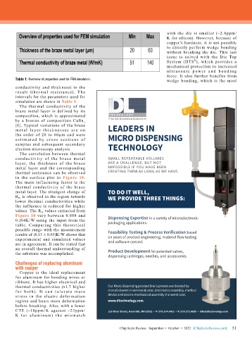
        Table 1: Overview of properties used for FEM simulation.              wedge bonding, which is the most
        conductivity and thickness) to the
        resu lt (t her mal resist a nce). T he
        intervals for the parameters used for
        simulation are shown in Table 1.
          The thermal conductivity of the
        braze metal layer is defined by its
        composition, which is approximated
        by a bronze of composition CuSn x
        [6]. Typical variations of the braze
        m e t a l l aye r t h ic k n e s s e s a r e o n   LEADERS IN
        the order of 20 to 60µm and were
        e s t i m a t e d b y  c r o s s s e c t io n s of   MICRO DISPENSING
        samples and subsequent secondary
        electron microscopy analysis.              TECHNOLOGY
          The correlation between thermal
        conduct iv it y  of  t he  br a ze  met al   SMALL REPEATABLE VOLUMES
        layer, the thick ness of the braze         ARE A CHALLENGE, BUT NOT
        metal layer and  the corresponding         IMPOSSIBLE IF YOU HAVE BEEN
        thermal resistance can be observed         CREATING THEM AS LONG AS WE HAVE.
        in the surface plot in  Figure 10.
        The main inf luencing factor is the
        thermal conductivity of the braze
        metal layer. The strongest change of       TO DO IT WELL,
        R th  is observed in the region towards    WE PROVIDE THREE THINGS:
        lower thermal conductivities while
        the inf luence is reduced for higher
        values. The R th  values extracted from
        Figure 10  vary between 0.088 and
        0.104K/W using the input from the          Dispensing Expertise in a variety of microelectronic
        table.  Comparing  this  theoretical       packaging applications.
        possible range with the measurement
        results of (0.13 ± 0.03)K/W shows that     Feasibility Testing & Process Verification based
        experimental and simulated values          on years of product engineering, material flow testing
        are in agreement. It can be stated that    and software control.
        an overall thermal understanding of
        the substrate was accomplished.            Product Development for patented valves,
                                                   dispensing cartridges, needles, and accessories.
        Challenges of replacing aluminum
        with copper
          Copper is the ideal replacement
        for aluminum for bonding wires or
        ribbons. It has higher electrical and
        thermal conductivities (x1.7 higher        Our Micro Dispensing product line is proven and trusted by
        fo r b o t h). It c a n t ol e r a t e m o r e   manufacturers in semiconductor, electronics assembly, medical
        st ress in the elastic defor mation        device and electro-mechanical assembly the world over.
        regime and bears more deformation          www.dltechnology.com.
        before breaking. Also, with a lower
        CTE (~18ppm/K against ~23ppm/              216 River Street, Haverhill, MA 01832  •  P: 978.374.6451  •  F: 978.372.4889  •  info@dltechnology.com
        K fo r a l u m i n u m) t h e m i s m a t c h


                                                                                                             51
                                                         Chip Scale Review   September  •  October  •  2022   [ChipScaleReview.com]  51

