Page 46 - Chip Scale Review_May June_2022-digital
P. 46
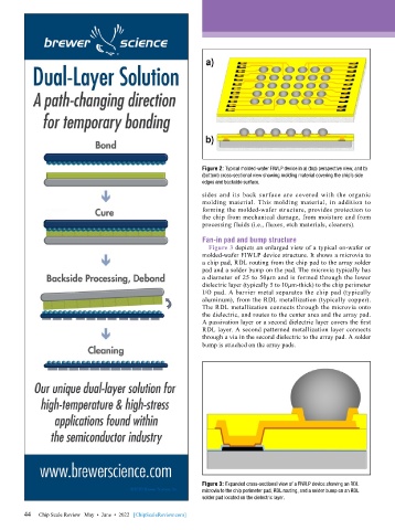
Figure 2: Typical molded-wafer FIWLP device in a) (top) perspective view, and b)
                                                             (bottom) cross-sectional view showing molding material covering the chip’s side
                                                             edges and backside surface.
                                                             sides and its back surface are covered with the organic
                                                             molding material. This molding material, in addition to
                                                             forming the molded-wafer structure, provides protection to
                                                             the chip from mechanical damage, from moisture and from
                                                             processing fluids (i.e., fluxes, etch materials, cleaners).
                                                             Fan-in pad and bump structure
                                                               Figure 3 depicts an enlarged view of a typical on-wafer or
                                                             molded-wafer FIWLP device structure. It shows a microvia to
                                                             a chip pad, RDL routing from the chip pad to the array solder
                                                             pad and a solder bump on the pad. The microvia typically has
                                                             a diameter of 25 to 50µm and is formed through the lower
                                                             dielectric layer (typically 5 to 10µm-thick) to the chip perimeter
                                                             I/O pad. A barrier metal separates the chip pad (typically
                                                             aluminum), from the RDL metallization (typically copper).
                                                             The RDL metallization connects through the microvia onto
                                                             the dielectric, and routes to the center area and the array pad.
                                                             A passivation layer or a second dielectric layer covers the first
                                                             RDL layer. A second patterned metallization layer connects
                                                             through a via in the second dielectric to the array pad. A solder
                                                             bump is attached on the array pads.


                                                             Figure 3: Expanded cross-sectional view of a FIWLP device showing an RDL
                                                             microvia to the chip perimeter pad, RDL routing, and a solder bump on an RDL
                                                             solder pad located on the dielectric layer.

        44   Chip Scale Review   May  •  June  •  2022   [ChipScaleReview.com]
        44

