Page 42 - Chip Scale Review_May June_2022-digital
P. 42
•  A heterogeneous integration of the
                                                                                  baseband chipset and AiP with heat
                                                                                  spreader/sink fabricated using the
                                                                                  chip-first with die face-down fan-out
                                                                                  process has been proposed.
                                                                                •  The chip-first with die face-up process
                                                                                  is for larger chip sizes (≤12mm x
                                                                                  12mm), smaller metal L/S (≥5μm)
                                                                                  RDL, and larger package sizes
                                                                                  (≤25mm x 25mm). Because of the
                                                                                  DAF process, there is no die shift
                                                                                  issue, which has been demonstrated
                                                                                  with an example.
                                                                                •  The chip-last process can be used
                                                                                  for very large chip sizes (≤20mm
                                                                                  x 20mm), ver y large  package
                                                                                  sizes (≤55mm x 55mm), and very
                                                                                  small  metal  L/S  (≥2μm)  RDLs
                                                                                  (the so-called fine-metal L/S RDL
                                                                                  substrate). A few examples of
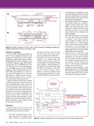
        Figure 10: a) TSMC’s AiP patent: US 10,312,112, June 4, 2019; b) Unimicron’s heterogeneous integration of   the heterogeneous integration of
        baseband and AiP patent: TW 1,209,218, November 1, 2020.                  multi-chip on fine-metal L/S RDL
                                                                                  substrate have been provided.
        Antenna-in-package                     formations, namely chip first with   •  With respect to chip-last with
          In [14], TSMC demonstrated that the   die face down, chip first with die   ultra-fine metal L/S (<2μm) RDL
        InFO_AiP for high-performance and      face up, and chip last or RDL first.   substrates, we can say this: before
        compact 5G millimeter-wave system    •  The chip-first with die face-down   the fine-metal L/S RDL substrate,
        integration is superior than that of solder-  package is for smaller chip sizes   one should first fabricate the ultra-
        bumped flip-chip AiP on substrate: 1) in   (≤5mm x 5mm), larger metal L/S   fine metal L/S RDL substrate as
        the 28GHz frequency range, InFO RDLs   (≥10μm) RDLs, and smaller package   shown in the US patent application
        transmission loss (0.175dB/mm) is 65%   sizes (≤10mm x 10mm). Because of   (Figure 11) by Unimicron.
        less than that on a flip-chip substrate   the small chip sizes and large metal     •  A heterogeneous integration of the
        trace (0.288dB/mm), and 2) in the 38GHz   L/S RDLs, the impact of die shift   application-specific IC (ASIC)/switch,
        frequency range, the transmission loss for   on  the manufacturing yield  is   EIC, and PIC on a fine-metal L/S RDL
        InFO RDLs (0.225dB/mm) is 53% less     small. A couple of examples of the   substrate fabricated by the chip-last
        than that (0.377dB/mm) on a flip-chip   heterogeneous integration of chips   fan-out process has been proposed.
        substrate trace. TSMC’s patent on InFO_  and mini-LEDs have been provided.
        AiP is shown in Figure 10a—it is a chip-
        first with die face-up fan-out process.
          Figure 10b shows the Unimicron patent
        of the heterogeneous integration of AiP
        and a baseband chipset using a chip-first
        with die face-down fan-out process. It
        can be seen that the radio frequency (RF)
        chip and the baseband chipset (modem
        application processor and the dynamic
        random access memory [DRAM]) are
        placed side-by-side with RDLs and
        coupled with the antenna patches. A heat
        spreader/sink is also proposed, which is
        almost impossible using a chip-first with
        die face-up fan-out process.

        Summary
          S o m e  i m p o r t a n t  r e s u l t s  a n d
        recommendations given the information
        presented are summarized as follows:

          •  The most important task in fan-
            out packaging is to fabricate the
            RDLs. There are at least three RDL   Figure 11: Unimicron’s future ultra-fine metal L/S RDL-substrate. US Patent filed on April 19, 2021.

        40
        40   Chip Scale Review   May  •  June  •  2022   [ChipScaleReview.com]

