Page 37 - Chip Scale Review_May June_2022-digital
P. 37
dispensing, compression molding, and
                                                                              then PMC are done. Then, the following
                                                                              are done: 1) backgrinding of the EMC
                                                                              to expose the Cu stud; 2) fabricating the
                                                                              RDLs; 3) and mounting the solder balls.
                                                                              Those processes are then followed by
                                                                              scanning a laser through the temporary
                                                                              glass carrier to the LTHC layer—the
                                                                              LTHC layer becomes powder, and the
                                                                              temporary glass carrier is then very easy
                                                                              to remove. Finally, the reconstituted
                                                                              wafer (with chips, EMC, RDLs, and
                                                                              solder balls) is diced into individual
                                                                              packages. There are three RDLs in
                                                                              each package and the minimum metal
                                                                              line width (L) and spacing (S) are 5μm.
                                                                              For detailed information on the design,
                                                                              materials, process, fabrication, and
                                                                              reliability of the chip-first with die face-
                                                                              up fan-out packaging, please see [4].
                                                                              TSMC’s integrated fan-out (InFO) [5]
                                                                              used for Apple’s application processor
                                                                              is one of the chip-first with die face-up
                                                                              fan-out processes.
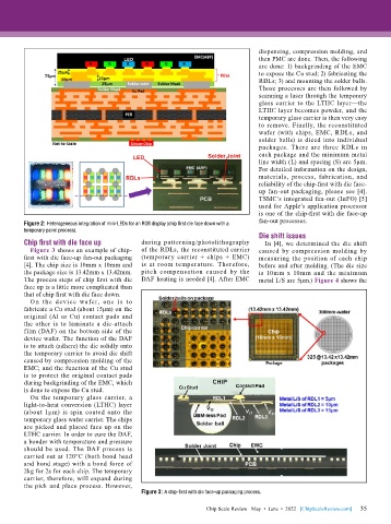
        Figure 2: Heterogeneous integration of mini-LEDs for an RGB display (chip first die face down with a
        temporary panel process).
                                                                              Die shift issues
        Chip first with die face up        during  patterning/photolithography   In [4], we determined the die shift
          Figure 3 shows an example of chip-  of the RDLs, the reconstituted carrier   caused by compression molding by
        first with die face-up fan-out packaging   (temporary carrier + chips + EMC)   measuring the position of each chip
        [4]. The chip size is 10mm x 10mm and   is at room temperature. Therefore,   before and after molding. (The die size
        the package size is 13.42mm x 13.42mm.   pitch compensation caused by the   is 10mm x 10mm and the minimum
        The process steps of chip first with die   DAF heating is needed [4]. After EMC   metal L/S are 5μm.) Figure 4 shows the
        face up is a little more complicated than
        that of chip first with die face down.
          On the device wafer, one is to
        fabricate a Cu stud (about 15μm) on the
        original (Al or Cu) contact pads and
        the other is to laminate a die-attach
        film (DAF) on the bottom side of the
        device wafer. The function of the DAF
        is to attach (adhere) the die solidly onto
        the temporary carrier to avoid die shift
        caused by compression molding of the
        EMC; and the function of the Cu stud
        is to protect the original contact pads
        during backgrinding of the EMC, which
        is done to expose the Cu stud.
          On the temporary glass carrier, a
        light-to-heat conversion (LTHC) layer
        (about  1μm)  is  spin  coated  onto  the
        temporary glass wafer carrier. The chips
        are picked and placed face up on the
        LTHC carrier. In order to cure the DAF,
        a bonder with temperature and pressure
        should be used. The DAF process is
        carried out at 120ºC (both bond head
        and bond stage) with a bond force of
        2kg for 2s for each chip. The temporary
        carrier, therefore, will expand during
        the pick and place process. However,
                                           Figure 3: A chip-first with die face-up packaging process.

                                                                                                             35
                                                               Chip Scale Review   May  •  June  •  2022   [ChipScaleReview.com]  35

