Page 34 - Chip Scale Review_May June_2022-digital
P. 34
Status and outlook for fan-out wafer/panel-level


        packaging


        By John H. Lau  [Unimicron Technology Corporation]
        T        h e  b ig g e s t  d i f fe r e n c e   less pad has been used for the solder   LEDs are red (R) (125 × 250 × 100µm),


                 between fan-out technology
                 and f lip-chip technology   ball, the Cu conductor layer of RDL2   green (G) (130 × 270 × 100µm), and
                                                                              blue (B) (130 × 270 × 100µm). The
                                           is thicker than that of RDL1. This is
        is that fan out needs to fabricate the   because of the Cu consumption due to   spacing among the RGB mini-LEDs is
        redistribution layers (RDLs), but flip   solder reflow and during operation.   80µm, the pixel-to-pixel spacing is also
        chip uses the substrate with RDLs.   For detailed information on the design,   ~80µm, and the pixel pitch is 625µm.
        There are at least three different   materials, process, fabrication, and   There are two RDLs in each package.
        formations of fan-out RDLs, namely: a)   reliability of the PCB assembly of the   A printed circuit board (PCB) (132mm
        chip first with die face down;  b) chip   heterogeneous integration package,   × 77mm) is designed and fabricated
        first with die face up; and c) chip last (or   please see [1,2].      for the drop testing that is done on the
        RDL first). In this brief article, recent   Figure 2 shows an example of   mini-LED package. Thermal cycling
        advances in fan-out are presented, such   heterogeneous integration of mini-light-  of the mini-LED surface mount device
        as: 1) RDL formations; 2) heterogeneous   emitting diodes (LEDs) for an RGB   (SMD) PCB assembly is also performed
        integration of the baseband chip and   display using chip-first with die face-  by a nonlinear temperature- and time-
        antenna-in-package (AiP); and 3)   down fan-out packaging [3]. The mini-  dependent finite-element simulation [3].
        heterogeneous integration of photonic
        integrated circuits (PIC) and electronic
        i nt eg r at ed ci rcu it s ( EIC). Some
        recommendations are also provided.
        Chip first with die face down
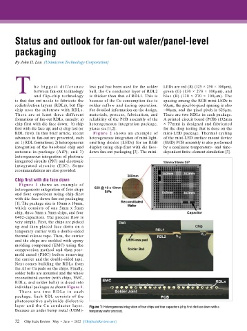
          Figure 1 shows an example of
        heterogeneous integration of four chips
        and four capacitors using chip-first
        with die face-down fan-out packaging
        [1]. The package size is 10mm x 10mm,
        which consists of one 5mm x 5mm
        chip, three 3mm x 3mm chips, and four
        0402-capacitors. The process flow is
        very simple. First, the chips are picked
        up and then placed face down on a
        temporary carrier with a double-sided
        thermal release tape. Then, the carrier
        and the chips are molded with epoxy
        molding compound (EMC) using the
        compression method and then post-
        mold cured (PMC) before removing
        the carrier and the double-sided tape.
        Next comes building the RDLs from
        the Al or Cu pads on the chips. Finally,
        solder balls are mounted and the whole
        reconstituted carrier (with chips, EMC,
        RDLs, and solder balls) is diced into
        individual packages as shown Figure 1.
          T h e r e a r e t wo R D L s  i n e a c h
        package. Each RDL consists of the
        photosensitive  polyimide  dielectric
        layer and the Cu  conductor  layer.   Figure 1: Heterogeneous integration of four chips and four capacitors (chip first die face down with a
        Because an under bump metal (UBM)-  temporary wafer process).

        32
        32   Chip Scale Review   May  •  June  •  2022   [ChipScaleReview.com]

