Page 29 - Chip Scale Review_May June_2022-digital
P. 29
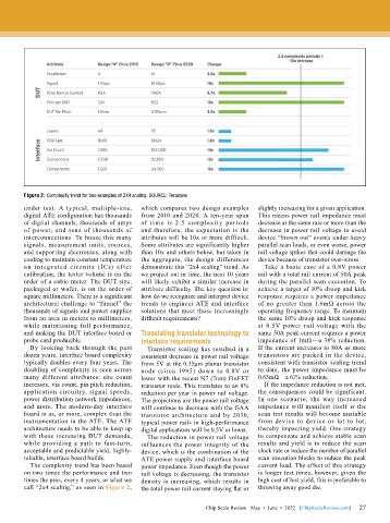
Figure 2: Complexity trend for two examples of 2X4 scaling. SOURCE: Teradyne
        under test. A typical, multiple-site,   which compares two design examples   slightly increasing for a given application.
        digital ATE configuration has thousands   from 2010 and 2020. A ten-year span   This means power rail impedance must
        of digital channels, thousands of amps   of time is 2.5 complexity periods   decrease at the same rate or more than the
        of power, and tens of thousands of   and therefore, the expectation is the   decrease in power rail voltage to avoid
        interconnections. To house this many   attributes will be 10x or more difficult.   device “brown out” events under heavy
        signals, measurement units, sources,   Some attributes are significantly higher   parallel scan loads, or even worse, power
        and supporting electronics, along with   than 10x and others below, but taken in   rail voltage spikes that could damage the
        cooling to maintain constant temperature   the aggregate, the design differences   device because of transistor over-stress.
        on integrated circuits (ICs) after   demonstrate this “2x4 scaling” trend. As   Take a basic case of a 0.8V power
        calibration, the tester volume is on the   we project out in time, the next 10 years   rail with a total rail current of 50A peak
        order of a cubic meter. The DUT size,   will likely exhibit a similar increase in   during the parallel scan execution. To
        packaged or wafer, is on the order of   attribute difficulty. The key question is:   achieve a target of 10% droop and kick
        square millimeters. There is a significant   how do we recognize and interpret device   response requires a power impedance
        architectural challenge to “funnel” the   trends to engineer ATE and interface   of no greater than 1.6mΩ across the
        thousands of signals and power supplies   solutions that meet those increasingly   operating frequency range. To maintain
        from an area in meters to millimeters,   difficult requirements?      the same 10% droop and kick response
        while maintaining full performance,                                   at 0.5V power rail voltage with the
        and making the DUT interface board or   Translating transistor technology to   same 50A peak current requires a power
        probe card producible.             interface requirements             impedance of 1mΩ—a 38% reduction.
          By looking back  through  the  past   Transistor scaling has resulted in a   If the current increases to 80A as more
        dozen years, interface board complexity   consistent decrease in power rail voltage   transistors are packed in the device,
        typically doubles every four years. The   from 5V at the 0.35µm planar transistor   consistent with transistor scaling trend
        doubling of complexity is seen across   node (circa 1995) down to 0.8V or   to date, the power impedance must be
        many different attributes: site count   lower with the recent N7 (7nm) FinFET   0.63mΩ—a 61% reduction.
        increases, via count, pin pitch reduction,   transistor node. This translates to an 8%   If the impedance reduction is not met,
        application circuitry, signal speeds,   reduction per year in power rail voltage.   the consequences could be significant.
        power distribution network impedances,   The projections are the power rail voltage   In one scenario, the way increased
        and more. The modern-day interface   will continue to decrease with the GAA   impedance will manifest itself is the
        board is as, or more, complex than the   transistor architecture and by 2030,   scan test results will become unstable
        instrumentation in the ATE. The ATE   typical power rails in high-performance   from device to device or lot to lot,
        architecture needs to be able to keep up   digital applications will be 0.5V or lower.  thereby impacting yield. One strategy
        with these increasing DUT demands,   The reduction in power rail voltage   to compensate and achieve stable scan
        while providing a path to fast-turn,   influences the power integrity of the   results and yield is to reduce the scan
        acceptable and predictable yield, highly-  device, which is the combination of the   clock rate or reduce the number of parallel
        reliable, interface board builds.  ATE power supply and interface board   scan execution blocks to reduce the peak
          The complexity trend has been based   power impedance. Even though the power   current load. The effect of this strategy
        on two times the performance and two   rail voltage is decreasing, the transistor   is longer test times, however, given the
        times the pins, every 4 years, or what we   density is increasing, which results in   high cost of lost yield, this is preferable to
        call “2x4 scaling,” as seen in Figure 2,   the total power rail current staying flat or   throwing away good die.


                                                                                                             27
                                                               Chip Scale Review   May  •  June  •  2022   [ChipScaleReview.com]  27

