Page 32 - Chip Scale Review_May June_2022-digital
P. 32
As an example of the discussion
                                                                              at the end of the previous paragraph,
                                                                              assume 10 probe pins, each nominally
                                                                              at  50mΩ,  and  the  DUT  requires  1V
                                                                              at 5A, for 0.5A per probe. In this
                                                                              case, the power dissipated per probe
                                                                              is I^2 * R = .05^2 * .5= 12.5mW. If
                                                                              one of the ten pins changes state from
                                                                              50mΩ  to  1Ω  (e.g.,  because  of  dirty
                                                                              needle tips), then in the  individual
                                                                              wide trace per VS case, the current
                                                                              per pin is still the same due to current
                                                                              sharing, and that pin goes to I^2 *
                                                                              R = .05^2 * 1= 250mW, compared to
                                                                              the 12.5mW design target. This is a
                                                                              1900% increase in power dissipation,
                                                                              which will likely damage pins. It is
                                                                              impractical to derate the nominal pin
                                                                              power rating to handle this increase.
                                                                                W hereas, in the common plane
                                                                              for the VS rail, the voltage on the
                                                                              interface and the DUT pad remains
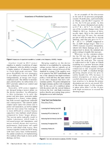
        Figure 4: Impedance of capacitors in parallel vs. transient current frequency. SOURCE: Teradyne  the same for each pin. The current
          A n o t h e r t r e n d i n DU T p owe r   Merging supplies on the device   is  redirected  to  the  9  pins  at  50mΩ
        supplies is smaller resolution of amps   interface is accomplished by connecting   resulting in a current increase from
        per channels, with the ability to merge   voltage sources that are typically set up   0.5A/pin to 0.55A/pin, which is 15mW
        a higher number of channels together   to equally share current between all the   compared to the or igi nal desig n
        to  reach  high  peak  currents.  This   channels in a group. If the supplies were   target of 12.5mW. A standard design
        gives f lexibility for test strategies   to be routed to the DUT individually and   derating should allow for pins to
        to test different sections of the DUT   one of the channels has high-resistance   safely handle the 20% increase in
        independently, or merge into larger   probes, it will still force the same current   power dissipation, or more, given
        combined rails. The ability to measure   as the other channels that have low-  careful  planning and  analysis.  The
        and control power in subsections of a   resistance probes. The power dissipated in   best practice is to derate the power
        DUT provides added test control and     the high-resistance probes will eventually   dissipation per pin to not exceed 50%
        data collection.                   fail. In the case of a combined plane   of the design target. In this example,
          Ty pically,  ATE  power  supplies   with the power rail, the current balances   it takes more than 3 of the 10 pins
        are merged using a power plane on   between the low- and high-resistance   with high resistances to exceed the
        the device interface. An alternative   probes thereby preventing large power   derating target.
        to t h is tech n ique is to split t he   dissipation on an individual pin.
        power rail into more, narrower paths
        compared to a fewer, wider paths,
        but with several significant tradeoffs
        and consequences. The narrow paths
        require more space for power rail to
        power rail separation, as well as added
        room for more sense line routings. It
        is more difficult to connect bypass
        capacitors into multiple small planes
        compared to fewer larger planes.
        The narrow paths typically result in
        higher inductance, which leads to
        increased power rail impedance, and
        worse overall droop and recovery
        performance. Each power rail could
        utilize individual wide traces, then
        connect together inside the DUT along
        with their sense lines. Unfortunately,
        the added complexity of implementing
        this method often leads to more probe
        damage, not less.
                                           Figure 5: Total test cost reduction summary. SOURCE: Teradyne

        30
        30   Chip Scale Review   May  •  June  •  2022   [ChipScaleReview.com]

