Page 30 - Chip Scale Review_May June_2022-digital
P. 30
Supporting DUT trends with ATE
        architecture
          The ATE and device interface board
        (DIB) architectures are critical to
        the ability to sufficiently test current
        and future devices. The following are
        examples of architectures that enable the
        DUT trends discussed in this article.
          Cleaner paths from instruments to
        DUTs and to application circuitry.
        A traditional interface board has
        instruments connecting to extremely
        dense “clusters” of function types
        (power, digital, analog, utility signals,
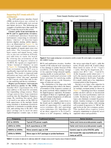
        etc.), as illustrated in Figure 3a. As
        site and channel counts increase, a
        large number of signals must cross over
        each other. The crossovers increase
        layer counts and signal losses, make
        site to site test correlation difficult,
        and add time to route the board.
        By rotating the orientation of the   Figure 3: Power supply routing layer comparison for: a) (left) a classic DIB; and b) (right) a next-generation
        instruments 90 degrees relative to   DIB. SOURCE: Teradyne
        the DUT, the signals are organized in   DUTs and application circuitry. Another   the series equivalent R and L, adds the
        ”strips,” instead of “clusters,” as seen   benefit of the reduced total capacitance   terms, Zl=jωL and Zr=R. Z total is these
        in Figure 3b. Consequently, the routing   is less damage to probes because of the   three terms in series. Z= R + 1/(jωC)
        from instrument to the DUT area is   possibility of the high energy storage   + (jωL). Solving for magnitude, |Z| =
        significantly improved into clean routing   of the capacitor being released rapidly,   square root {R^2 + [ωL – 1/(ωC)]^2}.
        channels. This results in improved route   causing needle or socket pin burn. Table   At the frequency point where (ωL) = 1/
        utilization per layer and the ability to   2 compares traditional solutions with   (ωC), the reactive terms cancel out, and
        implement a clean “site copy” approach   better solutions for satisfying stable   all that remains is the R term. Typically,
        to DUT layout, which then aids in site-  DUT voltages across a wide frequency   R is small, which sets a low impedance
        to-site matching and device correlation.  range of transient currents.  resonant point at that frequency.
          Higher-performance instruments     The elimination of the large-value bulk   Having a very large value capacitor in
        and delivery paths to the DIBs.    capacitor packages also reduces the chance   parallel with small value capacitors can
        Another DUT requirement the ATE    of resonances in the frequency response of   set multiple resonant points as shown in
        must address is the need for extremely   the power network when combined with   Figure 4. Operating near these resonant
        fast responding voltage sources. These   the high-frequency capacitors. Resonance   points can have adverse or inconsistent
        voltage sources have loop responses   can happen if there is a significant gap in   results on power performance and test
        reaching into the Megahertz frequency   the self-resonant frequencies of different   results. Reducing to fewer capacitor
        range. By reaching this speed, there   capacitor banks on the board.  types can eliminate resonant frequency
        is no need to use space on the DIB for   Capacitors and their connections to   points. Another strategy is to add many
        bulk capacitance in the multiple farads   the board can be simplified into a series   different capacitor values, with varying
        using tantalum or aluminum electrolytic   model of capacitance (C), equivalent   self-resonant frequencies, to “fill in” the
        capacitors to maintain acceptable droop,   series resistance (R), and equivalent   gap between the two resonance points.
        kick, and settling time at the DUT. This   series inductance (L). Impedance (Z)   This method often requires power
        space savings can be used for more   of an ideal capacitor is Zc=1/(jωC),   integrity simulation to properly select
        higher-frequency ceramic caps, or more   where ω is 2π* frequency. Adding in   capacitor values and quantities.


        Table 2: Comparison of solutions for satisfying stable DUT voltages across a wide frequency range of transient currents.

        28   Chip Scale Review   May  •  June  •  2022   [ChipScaleReview.com]
        28

