Page 39 - Chip Scale Review_May June_2022-digital
P. 39
the photoresist, using LDI and then
                                                                              developing the photoresist, and then
                                                                              using ECD to deposit the Cu. These
                                                                              steps are followed by stripping off the
                                                                              photoresist and etching off the TiCu
                                                                              seed layer to get the ML (ML2) of
                                                                              RDL2. Next comes slit coating a PID
                                                                              and LDI to get the DL (DL12) of RDL2.
                                                                              The same process steps are repeated to
                                                                              obtain the ML (ML1) and DL (DL01)
                                                                              of RDL1. Next comes sputtering the
                                                                              Ti/Cu, slit coating the photoresist, LDI
                                                                              and develop, and using ECD to deposit
                                                                              the Cu. Those steps are followed
                                                                              by stripping off the photoresist and
                                                                              etching off the TiCu to get the bonding
                                                                              pad (lead) for the chips. The last step
                                                                              in the fabrication of the RDL substrate
                                                                              immediately before the chips-to-
                                                                              subst rate bonding is the su rface
                                                                              finishing of the Cu bonding pads.
                                                                              Electroless palladium and immersion
                                                                              gold (EPIG) surface finishing is used.
                                                                              The fabrication of the fine-metal L/S
                                                                              RDL substrate is thereby completed.
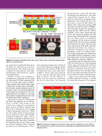
        Figure 6: Heterogeneous integration of three chips on a fine-metal L/S (2μm-minimum) RDL substrate using a   In parallel with the fabrication of the
        chip-last fan-out panel process.
                                                                              RDL-first substrate, the wafer bumping
        are much more complicated than those   electrochemical deposition (ECD) of   of the large and small chips with the
        of chip-first with face-up and face-  Cu is done following stripping off the   standard PVD and ECD Cu and solder
        down processes. The chip-last process   photoresist and etching off the Ti/Cu   process is performed. The next step is
        is meant for high-density and high-  to obtain the metal layer (ML) ML3   dicing the wafers into individual chips.
        performance (and therefore, higher   of RDL3. Those steps are followed   For all the chips, the bump consists of
        cost) applications.                by slit coating a PID and then using   the Cu pillar, Ni barrier, and SnAg cap.
          Figure 6 shows an example of     LDI to obt ai n the DL  (DL23) of    Now, we are ready to do the chips-
        heterogeneous integration of three chips   RDL3. The next steps are: sputtering   to-RDL substrate bonding. It should
        on a fine-metal L/S RDL-substrate [9,10].   the Ti/Cu seed layer, slit coating   be noted that, because of the support
        The size of the large chip is 10mm x
        10mm, and that of the smaller chip is 5mm
        x 7mm. There are three layers of the RDL-
        first substrate, and the minimum metal L/S
        is equal to 2μm. One practical application
        of heterogeneous integration is for the
        application processor chipset, i.e., the large
        chip could be an application processor and
        the small chips could be memories.
          The process steps for fabricating
        the RDL-first substrate are as follows.
        Fi rst,  a  LTHC  f il m  (1μ m)  is  slit
        coated on a temporary rectangular
        glass carrier (515mm x 510mm) and
        that step is followed by slit coating
        a photo-imageable dielectric (PID)
        for the solder mask (or passivation
        layer) dielectric layer (DL) DL3B,
        as shown in Figure 6. Then, a Ti/Cu
        seed layer is formed by physical vapor
        deposition (PVD). That step is followed
        by applying photoresist, then using
        laser direct imaging (LDI), followed   Figure 7: Heterogeneous integration of two chips on a hybrid substrate (a combination of the fine-metal L/S
        by photoresist development. Then,   RDL substrate using a chip-last fan-out panel process, and the build-up package substrate with the C4 solder
                                           bump and underfill).

                                                                                                             37
                                                               Chip Scale Review   May  •  June  •  2022   [ChipScaleReview.com]  37

