Page 38 - Chip Scale Review_May June_2022-digital
P. 38
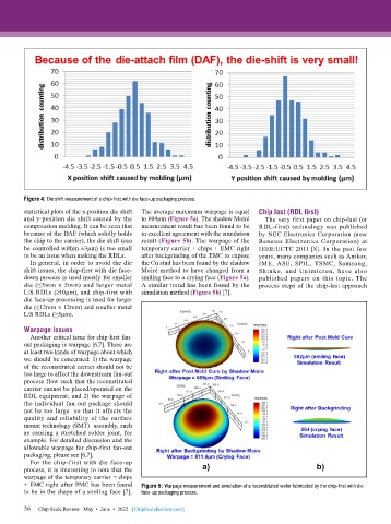
Figure 4: Die shift measurement of a chip-first with die face-up packaging process.

        statistical plots of the x-position die shift   The average maximum warpage is equal   Chip last (RDL first)
        and y-position die shift caused by the   to 609μm (Figure 5a). The shadow Moiré   The very first paper on chip-last (or
        compression molding. It can be seen that   measurement result has been found to be   RDL-first) technology was published
        because of the DAF (which solidly holds   in excellent agreement with the simulation   by NEC Electronics Corporation (now
        the chip to the carrier), the die shift (can   result (Figure 5b). The warpage of the   Renesas Electronics Corporation) at
        be controlled within ±3μm) is too small   temporary carrier + chips + EMC right   IEEE/ECTC 2011 [8]. In the past few
        to be an issue when making the RDLs.  after backgrinding of the EMC to expose   years, many companies such as Amkor,
          In general, in order to avoid the die   the Cu stud has been found by the shadow   IME, ASE, SPIL, TSMC, Samsung,
        shift issues, the chip-first with die face-  Moiré method to have changed from a   Shinko, and Unimicron, have also
        down process is used mostly for smaller   smiling face to a crying face (Figure 5a).   published papers on this topic. The
        die (≤5mm x 5mm) and larger metal     A similar trend has been found by the   process steps of the chip-last approach
        L/S RDLs (≥10μm), and chip-first with   simulation method (Figure 5b) [7].
        die face-up processing is used for larger
        die (≤12mm x 12mm) and smaller metal
        L/S RDLs (≥5μm).

        Warpage issues
          Another critical issue for chip-first fan-
        out packaging is warpage [6,7]. There are
        at least two kinds of warpage about which
        we should be concerned: 1) the warpage
        of the reconstituted carrier should not be
        too large to affect the downstream fan-out
        process flow such that the reconstituted
        carrier cannot be placed/operated on the
        RDL equipment; and 2) the warpage of
        the individual fan-out package should
        not be too large  so that it affects the
        quality and reliability of the surface
        mount technology (SMT)  assembly, such
        as causing a stretched solder joint, for
        example. For detailed discussion and the
        allowable warpage for chip-first fan-out
        packaging, please see [6,7].
          For the chip-first with die face-up
        process, it is interesting to note that the
        warpage of the temporary carrier + chips
        + EMC right after PMC has been found   Figure 5: Warpage measurement and simulation of a reconstituted wafer fabricated by the chip-first with die
        to be in the shape of a smiling face [7].   face-up packaging process.

        36   Chip Scale Review   May  •  June  •  2022   [ChipScaleReview.com]
        36

