Page 41 - Chip Scale Review_May June_2022-digital
P. 41
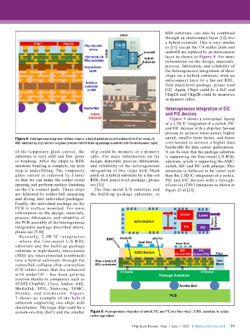
HDI substrate, can also be combined
                                                                              through an interconnect layer [12] into
                                                                              a hybrid substrate. This is very similar
                                                                              to [11] except the C4 solder joint and
                                                                              underfill are replaced by an interconnect
                                                                              layer as shown in Figure 8. For more
                                                                              information on the design, materials,
                                                                              process, fabrication, and reliability of
                                                                              the heterogeneous integration of three
                                                                              chips on a hybrid substrate with an
                                                                              interconnect layer by a fan-out RDL-
                                                                              first panel-level package, please read
                                                                              [12]. Again, Chip1 could be a SoC and
                                                                              Chip2A and Chip2B could be memories
                                                                              or memory cubes.

                                                                              Heterogeneous integration of EIC
                                                                              and PIC devices
                                                                                Figure 9 shows a conceptual layout
                                                                              of a 2.3D IC integration of a switch, PIC
                                                                              and EIC devices with a chip-last fan-out
                                                                              process to achieve lower power, higher
        Figure 8: Heterogeneous integration of three chips on a hybrid substrate (a combination of the fine-metal L/S   speed, smaller form factor, and lower
        RDL-substrate by chip-last fan-out panel process and the build-up package substrate with the interconnect layer).  cost needed to achieve a higher data
                                                                              bandwidth for data center applications.
        of the temporary glass carrier, the   chip could be memory or a memory   It can be seen that the package substrate
        substrate is very stiff and flat  prior   cube. For more information on the   is supporting the fine-metal L/S RDL
        to bonding. After the chips-to-RDL   design, materials, process, fabrication,   substrate, which is supporting the ASIC/
        substrate bonding is complete, the next   and reliability of the heterogeneous   switch, EIC and PIC with µbumps. This
        step is underfilling. The temporary   integration of two chips with 50µm   structure is believed to be lower cost
        glass  carrier  is  removed  by  a  laser   pitch on a hybrid substrate by a fan-out   than the 2.5D IC integration of a switch,
        so that we can make the solder resist   RDL-first panel-level package, please   PIC and EIC devices with a through-
        opening and perform surface finishing   see [11].                     silicon via (TSV) interposer as shown in
        on the Cu contact pads. Those steps   The fine-metal L/S substrate and   Figure 25 of [13].
        are followed by solder ball mounting   the build-up package substrate, or
        and dicing into individual packages.
        Finally, the individual package on the
        PCB is surface mounted. For more
        information on the design, materials,
        process, fabrication, and reliability of
        the PCB assembly of the heterogeneous
        integration package described above,
        please see [9,10].
          Re ce ntly, 2.3D IC i nt eg r at ion
        – where  the  f ine-metal  L/S  R DL
        substrate and the build-up package
        substrate or high-density interconnect
        (HDI) are interconnected (combined)
        into a hybrid substrate through the
        controlled collapse chip connection
        (C4) solder joints that are enhanced
        with underfill – has been gaining
        traction thanks to companies such as
        STATS ChipPAC, Cisco, Amkor, ASE,
        MediaTek,  SPIL,  Samsung,  TSMC,
        Sh i n ko, a nd Un i m ic ron.  F i g ure
        7 shows an example of the hybrid
        substrate supporting two chips with
        microbumps. The large chip could be a
        system-on-chip (SoC) and the smaller   Figure 9: Heterogeneous integration of switch, EIC, and PIC on a fine-metal L/S RDL substrate for a data
                                           center application.

                                                                                                             39
                                                               Chip Scale Review   May  •  June  •  2022   [ChipScaleReview.com]  39

