Page 45 - Chip Scale Review_May June_2022-digital
P. 45
Fan-in wafer-level packaging: any chip can be a flip chip!


        By Ray Fillion  [Fillion Consulting]

        I     n the November/December issue   smaller footprint, thinner devices   directly on a semiconductor wafer, and


              of  Chip Scale Review, seven
              advanced packaging technologies   for thinner, lighter products with   2) molded-wafer RDL processing, which
                                           increased functionality. Without fan-
                                                                              is processing on a reconstituted, molded
        were described [1]. The article covered   in technologies, personal electronic   wafer. Both of these FIWLP approaches
        embedded chip packaging (ECP), fan-in   products could not be as thin, as light   utilize 300mm semiconductor wafer
        wafer-level packaging (FIWLP), fan-out   and as small as they are, and still have   processing equipment.
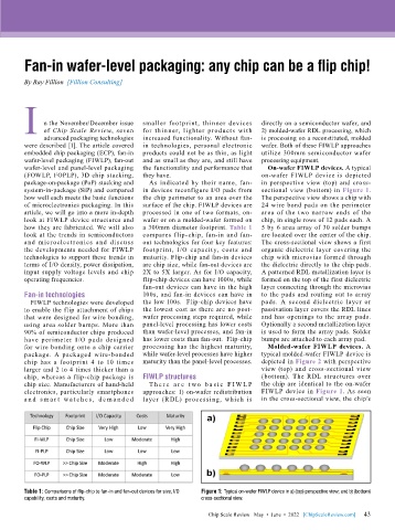
        wafer-level and panel-level packaging   the functionality and performance that   On-wafer FIWLP devices. A typical
        (FOWLP, FOPLP), 3D chip stacking,   they have.                        on-wafer FIWLP device is depicted
        package-on-package (PoP) stacking and   As indicated by their name, fan-  in perspective view (top) and cross-
        system-in-package (SiP) and compared   in devices reconfigure I/O pads from   sectional view (bottom) in Figure 1.
        how well each meets the basic functions   the chip perimeter to an area over the   The perspective view shows a chip with
        of microelectronics packaging. In this   surface of the chip. FIWLP devices are   24 wire bond pads on the perimeter
        article, we will go into a more in-depth   processed in one of two formats, on-  area of the two narrow ends of the
        look at FIWLP device structures and   wafer or on a molded-wafer formed on   chip, in single rows of 12 pads each. A
        how they are fabricated. We will also   a 300mm diameter footprint. Table 1   5 by 6 area array of 30 solder bumps
        look at the trends in semiconductors   compares flip-chip, fan-in and fan-  are located over the center of the chip.
        and  microelectronics  and  discuss   out technologies for four key features:   The cross-sectional view shows a first
        the developments needed for FIWLP   footprint, I/O capacity, costs and   organic dielectric layer covering the
        technologies to support these trends in   maturity. Flip-chip and fan-in devices   chip with microvias formed through
        terms of I/O density, power dissipation,   are chip size, while fan-out devices are   the dielectric directly to the chip pads.
        input supply voltage levels and chip   2X to 5X larger. As for I/O capacity,   A patterned RDL metallization layer is
        operating frequencies.             flip-chip devices can have 1000s, while   formed on the top of the first dielectric
                                           fan-out devices can have in the high   layer connecting through the microvias
        Fan-in technologies                100s, and fan-in devices can have in   to the pads and routing out to array
          FIWLP technologies were developed   the low 100s.  Flip-chip devices have   pads. A second dielectric layer or
        to enable the flip attachment of chips   the lowest cost as there are no post-  passivation layer covers the RDL lines
        that were designed for wire bonding,   wafer processing steps required, while   and has openings to the array pads.
        using area solder bumps. More than   panel-level processing has lower costs   Optionally a second metallization layer
        90% of semiconductor chips produced   than wafer-level processes, and fan-in   is used to form the array pads. Solder
        have perimeter I/O pads designed   has lower costs than fan-out.  Flip-chip   bumps are attached to each array pad.
        for wire bonding onto a chip carrier   processing has the highest maturity,   Molded-wafer FIWLP devices. A
        package. A packaged wire-bonded    while wafer-level processes have higher   typical molded-wafer FIWLP device is
        chip has a footprint 4 to 10 times   maturity than the panel-level processes.  depicted in Figure 2 with perspective
        larger and 2 to 4 times thicker than a                                view (top) and cross-sectional view
        chip, whereas a flip-chip package is   FIWLP structures               (bottom). The RDL structures over
        chip size. Manufacturers of hand-held   T h e r e a r e t w o b a s i c F I W L P   the chip are identical to the on-wafer
        electronics, particularly smartphones   approaches: 1) on-wafer redistribution   FIWLP device in Figure 1. As seen
        a nd s m a r t  w a t c h e s ,  d e m a nd e d   layer (RDL) processing, which is   in the cross-sectional view, the chip’s


        Table 1: Comparisons of flip-chip to fan-in and fan-out devices for size, I/O   Figure 1: Typical on-wafer FIWLP device in a) (top) perspective view; and b) (bottom)
        capability, costs and maturity.                      cross-sectional view.

                                                                                                             43
                                                               Chip Scale Review   May  •  June  •  2022   [ChipScaleReview.com]  43

