Page 48 - Chip Scale Review_May June_2022-digital
P. 48
pitches (55µm and below) have been
                                                                              demonstrated for flip-chip devices, they
                                                                              are only done where a flip-chip device is
                                                                              mounted onto a silicon substrate or onto a
                                                                              substrate having a similar low coefficient of
                                                                              thermal expansion (CTE) and are inherently
                                                                              planar. Tighter array pad pitches will
                                                                              require smaller diameter solder bumps with
                                                                              much lower solder height. On-wafer FIWLP
                                                                              devices can be fabricated with bump pitches
                                                                              down to 50µm and below when used on a
                                                                              silicon or other low coefficient of thermal
                                                                              expansion (CTE) substrate. Molded-wafer
                                                                              FIWLP devices are not dimensionally-
                                                                              stable enough to support these low solder
                                                                              bump pitches. Incorporation of Cu pillars
                                                                              on array pads would allow FIWLP devices
                                                                              to reduce solder bump height and, therefore,
                                                                              array pitch. Although most FIWLP devices
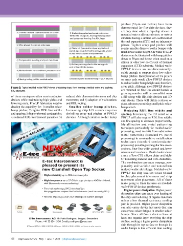
        Figure 5: Typical molded-wafer FIWLP device processing steps, from forming a molded-wafer and applying
        RDL structures.                                                       are mounted on fine-line circuit boards, a
                                                                              growing number will be assembled onto
        of these next-generation semiconductor   reduced chip placement tolerances and chip   a SiP along with flip-chip devices and 3D
        devices while maintaining high yields and   movement; and 6) adaption of via locations   chip stacks. These will utilize a silicon or
        lowering costs, FIWLP fabricators need to   and RDL routing.          glass substrate permitting small pitch solder
        develop the capability for: 1) smaller solder   Smaller solder bump pitches.   bump attach.
        bump pitches; 2) tighter RDL line widths   Increasing chip I/O counts requires   Reducing RDL line widths and
        and spacing; 3) higher thermal conductivity;   shrinking array pad pitches of FIWLP   spacing. Increasing the I/O count on a
        4) reduced RDL interconnect parasitics; 5)   devices. Although smaller solder bump   FIWLP will also require RDL line widths
                                                                              and line spacing to decrease proportionally.
                                                                              Metallization and metal patterning
                                                                              techniques particularly for molded-wafer
                                                                              processing, need to shift from subtractive
                                                                              metal patterning (standard PC panel
                                                                              processing) to semi-additive metallization
                                                                              techniques (standard semiconductor
                                                                              processing) providing rectangular line cross-
                                                                              sections, finer line width control and lower
                                                                              interconnect resistance. Molded wafers have
                                                                              a mix of low-CTE silicon chips and high-
                                                                              CTE molding material and RDL dielectrics.
                                                                              This combination can cause warpage, poor
                                                                              planarity and variable and nonuniform
                                                                              molded-wafer shrinkage. Molded-wafer
                                                                              FIWLP has chip location issues related
                                                                              to chip placement tolerances and chip
                                                                              movement after placement. All of these
                                                                              make going to finer features on molded-
                                                                              wafer FIWLP devices problematic.
                                                                                Higher power dissipation. Higher power
                                                                              dissipation chips can cause over heating of
                                                                              the chips and softening of organic materials
                                                                              unless a low thermal resistance cooling
                                                                              path is provided. Higher power dissipation
                                                                              can also cause device hot spots that can
                                                                              exacerbate solder fatigue in smaller solder
                                                                              bumps. Since all fan-in devices have at
                    E-Tec Interconnect  AG, Mr. Pablo Rodriguez,  Lengnau Switzerland  least one organic layer overlying the chip
                        Phone : +41 32 654 15 50, E-mail: p.rodriguez@e-tec.com  surface, cooling a higher power dissipation
                                                                              chip through its top surface or through its
                                                                              solder bumps is less efficient than cooling


        46   Chip Scale Review   May  •  June  •  2022   [ChipScaleReview.com]
        46

