Page 47 - Chip Scale Review_May June_2022-digital
P. 47
FIWLP processes
          The processing steps used to convert
        a chip designed for wire bonding into
        a FIWLP are nearly identical for both
        on-wafer processing and molded-wafer
        processing. The exceptions are the
        processing steps used to fabricate the
        molded wafer. Once the molded wafer is
        complete, exactly the same processing
        steps, processing equipment and processing
        materials are used by both.
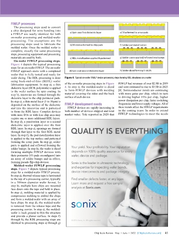
          On-wafer FIWLP processing steps.
        Figure 4 depicts the typical processing
        steps for an on-wafer FIWLP. The on-wafer
        FIWLP approach starts with a completed
        wafer that is fully tested and ready for
        wafer dicing. The RDL processing is done   Figure 4: Typical on-wafer FIWLP device processing steps forming RDL structures on a wafer.
        using back-end-of-line (BEOL) wafer
        fabrication equipment. In step a), a thin   of the on-wafer processing steps in Figure   FIWLP had revenues of over $2.5B in 2019
        dielectric layer (BCB, polyimide) is applied   4. In step i), the molded-wafer is diced   and were estimated to rise to $3.5B in 2025
        to the wafer surface by spin coating. In   to form FIWLP devices with molding   [4]. Semiconductor trends are continuing
        step b), microvias are formed through the   material covering the sides and the back   with more gates per chip, which in turn
        dielectric layer to the chip perimeter pads.   surface of each device.  is driving higher I/Os per chip, higher
        In step c), a thin metal layer (5 to 10µm) is                         power dissipation per chip, faster switching
        deposited on the surface of the dielectric   FIWLP development needs  frequencies and lower supply voltages. All of
        and into the microvias and is patterned   FIWLP devices are rapidly increasing in   these trends affect the FIWLP requirements
        to form the RDL layer. Complex devices   both number of devices shipped and total   in the coming years. In order to extend
        with more I/Os or with less chip area may   market value. Yole reported in 2020 that   FIWLP technologies to meet the needs
        require one or more additional RDL layers.
        In step d), a passivation layer or a second
        dielectric layer is applied over the first
        RDL layer. In step e), openings are formed
        through that layer to the first RDL metal
        layer. In step f), the pad metallization layer
        is applied to the top surface and patterned
        forming the array pads. In step g), solder
        paste is applied and reflowed forming the
        solder bumps. In step h), the wafer is diced
        forming multiple FIWLP devices with
        their perimeter I/O pads reconfigured into
        an array of solder bumps and in effect,
        forming pseudo flip-chip devices.
          Molded-wafer FIWLP processing
        steps. Figure 5 depicts typical processing
        steps for a molded-wafer FIWLP process.
        In step a), thermal release tape is laminated
        to the top of a processing carrier, typically
        in a 300mm diameter wafer format. In
        step b), multiple bare chips are mounted
        face down onto the tape and held in place.
        In step c), molding material is applied by
        compression molding to embed the chips
        and form a molded-wafer with an array of
        bare chips. In step d), the molded-wafer
        is removed from the release tape and the
        processing carrier. In step e), the molded-
        wafer is back ground to thin the structure
        and provide a planar surface. In steps f)
        through h), the RDL processing steps are
        identical to processing steps a) through g)


                                                                                                             45
                                                               Chip Scale Review   May  •  June  •  2022   [ChipScaleReview.com]  45

