Page 53 - Chip Scale Review_May June_2022-digital
P. 53
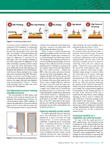
Figure 2: Clip sintering assembly process.
        is because of the coefficient of thermal   with the most commonly used being paste   After printing, the next assembly step is
        expansion (CTE) mismatch. To understand   and film—based on our observation with   nitrogen drying (see Figure 2, (C)).
        this importance, we can look at the CTE   HPE package developer end users.   The purpose of drying is to remove
        between the semiconductor die and metal   Figure 2 shows a typical clip pressure   the solvent within the printed paste. A
        clip. For example, if the semiconductor die   sintering assembly process that starts with   properly dried printed paste increases
        is made from silicon carbide with a CTE   the application of paste onto a substrate via   the  paste evenness and  firmness  to
        range of 3-4ppm per °C, and the CTE for   a custom-designed and fabricated stencil.   avoid paste spluttering or roll-up during
        clip copper with a few microns of plating on   The challenges faced during printing are to   clip placement. The last step of the clip
        its surface ranges from 16-18ppm per °C, the   avoid overprinting and smearing, as well as   sintering assembly process is pressure
        order of thermal expansion would be about   having to deal with the need for a two-step   sintering, where the two connection
        4 to 5 times the stress differential. If this   printing process. Printing is performed in   points – namely the source pad area and
        stress differential for the clip sintering is not   two separate steps because the clip attached   the top of the semiconductor chip – are
        designed with sufficient stress relief features,   has a two-ended location – namely the   pressure sintered with metal stamps.
        such stresses during thermal cycle testing   DBC, where the source pad area is located   Optimal stamp design is critical within
        may lead to breakage of the HPE. Therefore,   and the top of the semiconductor chip – to   the sintering tool to ensure sintering
        designs of stress relief features play a   complete the flow of electrical current. The   pressure is evenly applied onto the
        crucial role in reducing the interfacial stress   printed area where the clip will be attached   interconnection of the clip and its contact
        between the copper clip and semiconductor   is a fraction of the area of the total die size.   point, i.e., the source pad and the top
        chip metallization.  Figure 1 shows   There exists a height difference between   of the die. After the pressure sintering,
        some potential ways to reduce the stress    the source pad area and the substrate,   the quality of the sintered clip bond is
        because of CTE mismatch.           therefore, merging a two-step printing into   characterized by automated shearing or
                                           a single step would lead to insufficient   peel testing. The testing method employed
        Clip interconnect pressure sintering   printing pressure on at least one of the   is dependent on the design and size of
        assembly processes                 connecting points. Furthermore, fabricating   the clip. If the thickness of the clip is
          The clip assembly for HPE begins with   a 3D stencil would be a challenge for a   sizable for the shear tool to contact during
        printing of the sintered material onto the   single-print process. The first printing is   shearing, it will be used to evaluate the
        substrate. The example shown in Figure 1 is   performed on the DBC, which we term   clip bond force, otherwise peeling of the
        a direct-bonded copper (DBC) substrate. It   here as the first connection on the source   clip would be the alternative—which is
        requires the application of pressure sintering   pad area (A), and the second printing (B) is   most commonly used. Scanning acoustic
        paste to form a bond with the metal clip.   performed on top of the semiconductor top   microscopy will be employed to check for
        The sintering paste comes in many formats,   as shown in Figure 2.    voiding, delamination, and the uniformity
                                                                              of  the  pressure  of  the  completed
                                           Exploring optimally-printed results  sintered bond.
                                             To obtain optimally-printed sintering
                                           paste, the following factors must be   Using local facilities for a
                                           optimized: 1) paste viscosity at room   compatible clip sintering process
                                           temperature, 2) paste mixing and     To cope with the rapid growth of
                                           rollability, 3) printing speed, 4) printing   HPE applications, the manufacturing
                                           force, 5) printing direction, 6) stencil   requirements of the whole production line
                                           frame spring force, and 7) squeegee   should be considered. The clip sintering
                                           release speed and distance. Figure 3   process for HPE needs to be compatible with
                                           demonstrates the difference between   all the upstream and downstream processes.
                                           a poor printing outcome versus a good   Therefore, many manufacturers today are
                                           printing outcome for clip sintering, if   looking for local facilities to speed up the
                                           printing parameters are not optimized.   development processes and time to market.
        Figure 3: Difference between poor and good printing.

                                                                                                             51
                                                               Chip Scale Review   May  •  June  •  2022   [ChipScaleReview.com]  51

