Page 30 - Chip Scale Review_March April_2022-digital
P. 30
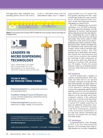
ECP approaches, other component types,   could be embedded along with the   cross-sectional view of a typical COF
        including passive devices and sensors,   semiconductor chips. Figure 2 depicts a   ECP module showing two bare chips
                                                                              of differing thicknesses and a passive
                                                                              device, all interconnected with a two-
                                                                              layer overlay interconnection structure
                                                                              and topside area array I/Os [3].
                                                                                The COF technology has several key
                                                                              advantages over the HDI technology.
                                                                              The most important advantage was the
                                                                              elimination of excessive chip movement
        Figure 2: Cross-sectional view of a typical COF ECP module with two overlay layers connecting two chips and   during chip placement and chip adhesive
        one passive device.                                                   cure, eliminating the need to adapt to
                                                                              the locations of the microvias and metal
                                                                              patterning. This feature makes it fully
                                                                              compatible with mask-based photo-
                                                                              patterning and volume scaled up to large-
                                                                              panel processing. Another advantage was
                                                                              the elimination of the custom and costly
                                                                              ceramic carrier with its mechanically-
             LEADERS IN                                                       machined chip cavities. The COF
                                                                              structure had a much flatter top surface
             MICRO DISPENSING                                                 that allowed fine interconnections and
                                                                              a much thinner structure that enabled
             TECHNOLOGY                                                       the mounting of other components on
                                                                              the top surface while also allowing the
                                                                              stacking of multiple COF substrates
             SMALL REPEATABLE VOLUMES                                         into 3D modules. Finally, the molded
             ARE A CHALLENGE, BUT NOT                                         substrate readily accommodated thermal
             IMPOSSIBLE IF YOU HAVE BEEN                                      structures under high-power dissipation
             CREATING THEM AS LONG AS WE HAVE.                                chips [4].
                                                                              ECP structures
                                                                                All ECP modules have a number of
             TO DO IT WELL,                                                   common structural features. First, bare
                                                                              chips and other devices are encased
             WE PROVIDE THREE THINGS:                                         in organic material covering the four
                                                                              sides and generally, the back surface of
                                                                              each device forming the ECP substrate.
                                                                              A low dielectric constant polymer
             Dispensing Expertise in a variety of microelectronic             overlays the components and the molded
             packaging applications.                                          substrate and forms the first dielectric
                                                                              layer. Microvias are formed through the
             Feasibility Testing & Process Verification based                 dielectric to the chip pads and to other
             on years of product engineering, material flow testing           component contacts. A thin, patterned
             and software control.                                            metal layer is formed on the top surface
                                                                              and into the microvias to the chip pads.
             Product Development for patented valves,                         A typical ECP module would have at
             dispensing cartridges, needles, and accessories.                 least one additional interconnect layer.
                                                                              The key feature of all ECP structures
                                                                              is the direct metallurgical connection
                                                                              of the interconnect metallization to
                                                                              the chip pads, thereby eliminating the
                                                                              parasitics associated with wire bonds
             Our Micro Dispensing product line is proven and trusted by       and solder bumps.
             manufacturers in semiconductor, electronics assembly, medical
             device and electro-mechanical assembly the world over.           ECP advantages
             www.dltechnology.com.                                              As mentioned above, a key advantage
                                                                              of ECP is its low interconnection
                                                                              parasitics. ECP structures lower chip-to-
             216 River Street, Haverhill, MA 01832  •  P: 978.374.6451  •  F: 978.372.4889  •  info@dltechnology.com
                                                                              chip parasitics by an order of magnitude

        28   Chip Scale Review   March  •  April  •  2022   [ChipScaleReview.com]
        28

