Page 31 - Chip Scale Review_March April_2022-digital
P. 31
verses flip-chip structures, and by two
        orders of magnitude verses wire bonds
        use in traditional MCMs. As shown in
        Table 1, the interconnection parasitics
        of ECP microvias that connect directly
        to the chip pads are less than 0.01nH
        of  inductance,  less  than  0.001pF  of
        capacitance, and less than 1.0mohms
        of resistance [5]. These low parasitics
        per m it  faster  clock rates,  faster
        switching, reduced line noise, and lower
        interconnect losses.
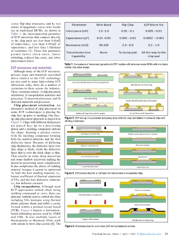
                                           Table 1: Comparisons of interconnect parasitics for ECP modules with microvias verses MCMs with wire bonds
        ECP processes and materials        and flip-chip solder bumps.
          Although many of the ECP structures,
        process steps and materials described
        above relative to the COF technology
        are also used by many high-volume ECP
        fabricators today, there are a number of
        variations in these across the industry.
        These variations include: 1) chip placement
        orientation; 2) encapsulation materials and
        processes; 3) microvia processes; and 4)
        dielectric materials and processes.
          Chip placement  orientation.  An
        alternative method of chip placement in
        some ECP technologies is placing the
        chip face up prior to molding. One face-
        up chip placement approach is depicted in   Figure 3: ECP face-up chip placement processing steps with both deep and shallow microvias to chips with
        Figure 3. Chips with different thicknesses   differing thicknesses.
        are placed face up  on a  processing
        platen and a molding compound embeds
        the chips, forming a molded carrier
        with the molding compound forming
        both the molded substrate and the first
        dielectric layer. Because of differing
        chip thicknesses, the dielectric layer over
        thin chips is thick, while the dielectric
        layer that is over the thick chips is thin.
        This results in some deep microvias
        and some shallow microvias making the
        microvia processing more complicated.
        It also complicates the choice of molding
        material because it cannot be optimized
        for both the best molding material, i.e.,   Figure 4: ECP process steps for a multilayer laminate process to encapsulate chips.
        lowest coefficient of thermal expansion
        (CTE), and the best dielectric material,
        i.e., low dielectric constant.
          Chip encapsulation. Although most
        ECP approaches embed chips using
        molding compound or resin, there are
        alternate methods used to embed the chips
        including film laminate using thermal
        plastic polymer sheets and within a cavity
        formed within a printed circuit board
        (PCB). Figure 4 depicts a lamination-
        based embedding process used by AT&S
        and TDK. It uses multiple layers of
        thermoplastic or thermoset films, each
        with cutouts to form chip cavities [6]. The
                                           Figure 5: Processing steps for a one-layer, ECP overlay lamination process.

                                                                                                             29
                                                             Chip Scale Review   March  •  April  •  2022   [ChipScaleReview.com]  29

