Page 32 - Chip Scale Review_March April_2022-digital
P. 32
chips are placed face down in the cavities   be embedded within a multilayer PCB.   high-cost laser to ablate microvias, a
        and a top film without cutouts is applied   As depicted in Figure 6, a chip cavity is   photo-definable overlay dielectric is used
        over the stack-up covering the chips in the   formed in a double-sided PCB with plated   that can be photo-defined by mask-based
        cavities. Standard lamination processing   through-holes (PTHs). A bare chip is placed   photo-processing. Another approach is
        steps with heat and pressure are used to   face down in the cavity and the cavity is   to apply and photo-pattern a hard mask
        soften the dielectric layers and reflow the   filled with molding material. Then, thin   forming openings at the microvias’
        resin around the chips, embedding them   dielectric layers are applied to both sides   locations and form the microvias by
        and bonding the layers together. Another   of the PCB and standard via formation,   chemical etch or plasma etch.
        laminate-based process utilizes one thick   metallization and patterning form double-  Thermal performance. Because all
        flowable thermoplastic organic film to   sided fine-line interconnect structures   ECPs are essentially a molded plastic
        embed thinned chips. Figure 5 depicts   directly connecting to the chip pads.  package, it might be assumed that ECPs
        a simple lamination process where one   Via formation. The predominant   would inherently have poor thermal
        thermoplastic film is draped over the chips.   method used to form ECP microvias in   performance. That is generally true for
        Then, a vacuum is pulled below the film   the overlay dielectric layers is by laser   a fully-encapsulated module without
        and heat and pressure are applied to the top   ablation—effectively vaporizing the   a direct high ther mal conduction
        of the film, which causes the organic film to   dielectric material and forming microvias   pathway to a heat sink. ECP fabricators
        encase the chips and form the first dielectric   with sloped sidewalls, optimized for   have addressed the issue of thermal
        layer. This process is generally applicable   microvia metallization. In some ECP   performance  of  their  processes  by
        to low I/O modules. Finally, chips can also   technologies, in order to avoid using a   providing a low thermal resistance path
                                                                              for higher power dissipation chips. There
                                                                              are two main approaches to improve ECP
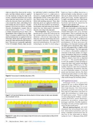
                                                                              thermal performance. The first approach
                                                                              is to attach a thermally-conductive
                                                                              structure to the back surface of a high-
                                                                              power dissipation chip prior to molding
                                                                              and then use a thermal interface material
                                                                              (TIM) to attach a heat sink as depicted
                                                                              in Figure 7. The second approach is
                                                                              to thin the module by back grinding to
                                                                              expose the chip’s back surface and attach
                                                                              a heat sink using a TIM (Figure 8). This
                                                                              method, however, does have drawbacks
                                                                              if the high-power dissipation chip has
                                                                              an active backside contact. In vertical
                                                                              power and microwave devices, the chip’s
                                                                              electrical ground contact is on the chip’s
        Figure 6: Process steps for embedding chips inside a PCB.             back surface. Back grinding to expose the
                                                                              chip could damage the backside contact.
                                                                              ECP application areas
                                                                                A lt hou g h E C Ps a r e ge n e r a l ly
                                                                              targeted for use in those modules that
                                                                              have only a few chips (say, 3-5, or so),
                                                                              their high density, low interconnect
                                                                              parasitics and low processing costs
                                                                              have led ECP fabricators and users to
                                                                              apply the technology to a wide array
        Figure 7: ECP module with thermal spacer directly attached to the back surface of a high-power dissipation   of application areas. These include
        chip and backside heat sink.                                          mixed analog/digital modules, sensors,
                                                                              control electronics, power electronics,
                                                                              photonics, microwave, single-chip
                                                                              packages and thin, flexible modules.
                                                                              Examples of some of these application
                                                                              areas are discussed below.
                                                                                Mixed analog/digital. All ECP
                                                                              structures that we reviewed have very
                                                                              low interconnect parasitics and can
                                                                              bring a matched transmission line all
                                                                              the way to the  chip pads as shown
        Figure 8: EP module with one high-dissipation chip with its back surface exposed by back grinding and with   earlier in Table 1. Because of this, ECP
        an attached heat sink.

        30
        30   Chip Scale Review   March  •  April  •  2022   [ChipScaleReview.com]

