Page 35 - Chip Scale Review_March April_2022-digital
P. 35
References
                                                                                1.  R .  F i l l i on ,  “ A dv a nc e d
                                                                                  m ic r o ele c t r o n ic s  p a ck a g i n g
                                                                                  technologies and their performance,”
                                                                                  Chip Scale Review, Nov/Dec 2021,
                                                                                  pp. 10-17.
                                                                                2. R. O. Carlson, et al., “A high
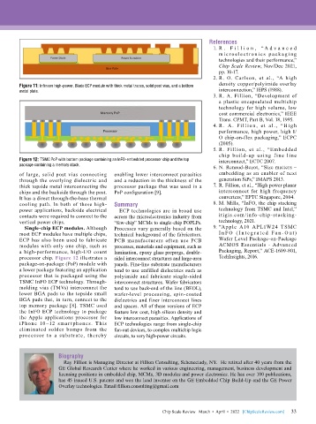
        Figure 11: Infineon high-power, Blade ECP module with thick metal traces, solid post vias, and a bottom   density copper/polyimide overlay
        metal plate.                                                              interconnection,” IEPS (1988).
                                                                                3. R. A. Fillion, “Development of
                                                                                  a plastic encapsulated multichip
                                                                                  technology for high volume, low
                                                                                  cost commercial electronics,” IEEE
                                                                                  Trans. CPMT, Part B, Vol. 18, 1995.
                                                                                4. R . A . Fi l l io n , e t  a l ., “ H ig h
                                                                                  performance, high power, high I/
                                                                                  O chip-on-flex packaging,” ECPC
                                                                                  (2005).
                                                                                5. R. Fillion, et al., “Embedded
                                                                                  chip build-up using f ine line
        Figure 12: TSMC PoP with bottom package containing an InFO-embedded processor chip and the top   interconnect,” ECTC 2007.
        package containing a memory stack.                                      6. N. Renaud-Bezot, “Size matters –

        of large, solid post vias connecting   enabling lower interconnect parasitics   embedding as an enabler of next
        through the overlying dielectric and   and a reduction in the thickness of the   generation SiPs,” IMAPS 2013.
        thick topside metal interconnecting the   processor package that was used in a   7.  R. Fillion, et al., “High power planar
        chips and the backside through the post.   PoP configuration [9].         interconnect for high frequency
        It has a direct through-the-base thermal                                  converters,” EPTC Singapore, 2004.
        cooling path. In both of these high-  Summary                           8. M. Mills, “InFO, the chip stacking
        power applications, backside electrical   ECP technologies are in broad use   technology from TSMC and Intel,”
        contacts were required to connect to the   across the microelectronics industry from   itigis.com/info-chip-stacking-
        vertical power chips.              “few-chip” MCMs to single-chip FOPLPs.   technology, 2021.
          Single-chip ECP modules. Although   Processes vary generally based on the   9. “Apple A10 A PL1W24 TSMC
        most ECP modules have multiple chips,   technical background of the fabricators.   I n F O  ( I n t e g r a t e d Fa n - O u t)
        ECP has also been used to fabricate   PCB manufacturers often use PCB     Wafer Level Package-on-Package
        modules with only one chip, such as   processes, materials and equipment, such as   ACMOS Essentials - Advanced
        a high-performance, high-I/O count   lamination, epoxy glass prepregs, double-  Packaging, Report,” ACE-1609-801,
        processor chip. Figure 12 illustrates a   sided interconnect structures and large-area   TechInsights, 2016.
        package-on-package (PoP) module with   panels. Fine-line substrate manufacturers
        a lower package featuring an application   tend to use unfilled dielectrics such as
        processor that is packaged using the   polyimide and fabricate single-sided
        TSMC InFO ECP technology. Through-  interconnect structures. Wafer fabricators
        molding vias (TMVs) interconnect the   tend to use back-end of the line (BEOL),
        lower BGA pads to the topside small   wafer-level processing, spin-coated
        BGA pads that, in turn, connect to the   dielectrics and finer interconnect lines
        top memory package [8]. TSMC used   and spaces. All of these versions of ECP
        the InFO ECP technology to package   feature low cost, high silicon density and
        the Apple applications processor for   low interconnect parasitics. Applications of
        iPhone 10 –12 smar t phones. This   ECP technologies range from single-chip
        eliminated solder bumps from the   fan-out devices, to complex multichip logic
        processor  to  a  substrate,  thereby   circuits, to very high-power circuits.


                       Biography
                         Ray Fillion is Managing Director at Fillion Consulting, Schenectady, NY.  He retired after 40 years from the
                       GE Global Research Center where he worked in various engineering, management, business development and
                       licensing positions in embedded chip, MCMs, 3D modules and power electronics. He has over 100 publications,
                       has 45 issued U.S. patents and was the lead inventor on the GE Embedded Chip Build-Up and the GE Power
                       Overlay technologies. Email fillion.consulting@gmail.com


                                                                                                             33
                                                             Chip Scale Review   March  •  April  •  2022   [ChipScaleReview.com]  33

