Page 38 - Chip Scale Review_March April_2022-digital
P. 38
large-size TSV interposers very expensive.
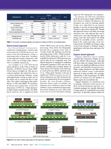
                                                                                In contrast, the TSV-less embedded
                                                                              multi-die interconnect bridge (EMIB) from
                                                                              Intel shown in Figure 6b addresses the
                                                                              interposer size issue by utilizing smaller
                                                                              bridge dies embedded in an organic
                                                                              package to provide localized high-density
                                                                              wiring to connect dies together [8]. Though
                                                                              this approach reduces cost while increasing
                                                                              interposer size, only adjacent dies can be
                                                                              connected to each other through the edges
                                                                              facing each other and requires two bump
                                                                              pitches for assembly (coarse- and fine-
        Table 1: Comparison of material properties and physical dimensions of different core material options.  pitch at the center and edge of the die,
                                                                              respectively). In EMIB, the bridges range
        Silicon-based approach             65nm-CMOS back end of line (BEOL)   in size from 2x2mm  to 8x8mm  using 4
                                                                                                        2
                                                                                               2
          I n  s i lic o n - b a s e d  i n t er p o s er s ,   processing. This allows for lithography   metal layers with 2µm lines and spaces for
        traditional complementary metal-oxide   ground  rules  ranging  from  1µm  to   the RDL.
        semiconductor (CMOS) processes are   <0.5µm [17,18]. The dielectric used for the
        used to form the high-density wiring to   interconnections is SiO 2 . While extreme-  Organic-based approach
        interconnect dies to each other. Variations   low-K (ELK) dielectrics with D k <3 are   Organic substrates can be further
        of this approach include interposers with   available for advanced CMOS processes on   classified into interposers (Figure 6c) and
        TSVs or the use of bridge chips without   silicon, they are not commonly used. The   fan-out (Figure 6d) packages. Although
        TSVs to establish connectivity.    silicon interposer is matched in coefficient   both these types use organic material as the
          An example of a 2.5D TSV-based   of thermal expansion (CTE) with the die,   core, there are significant differences in their
        silicon interposer is the Chip on Wafer on   thereby enabling fine assembly pitches of   structure and manufacturing processes.
        Substrate  (CoWoS ) process from TSMC   35µm using micro-bumps while attaching   While organic interposers and high-density
                       ®
        [16] as shown in Figure 6a. This process   to a ball grid array (BGA) substrate using   substrates follow a more conventional
        connects multiple fine-pitch bare dies to   C4 at ~130µm pitch. Because of the use of   approach of chip assembly after package
        a coarser-pitch package substrate, along   traditional CMOS processes, the size of   construction, in fan-out packages, the RDL
        with high-density wiring on either side of   silicon interposers are often limited by the   and IOs are formed over the molded, or
        the silicon core to connect the dies to each   reticle size supported by the semiconductor   fanout, region of a reconstituted die.
        other. Two critical technologies that enable   foundry. So, even though a 300mm-  Organic laminates are extensively used
        this are: 1) TSV, and 2) RDL. The advances   diameter silicon wafer is available, the   as package substrates today because of
        in Bosch processing have scaled the   interposer size is limited to areas less than   their electrical properties and low cost.
                                                  2
        dimensions of TSVs to <20µm diameter   1600mm  unless nontraditional approaches   Laminate packages are typically fabricated
        in high-volume manufacturing. The RDL   like reticle stitching are used, which adds   in large panels by sequentially processing
        layers, however, are re-engineered from   to the cost of silicon fabrication making   each layer of thin-film polymer dielectric


        Figure 6: Schematics of various approaches for heterogeneous integration.

        36   Chip Scale Review   March  •  April  •  2022   [ChipScaleReview.com]
        36

