Page 43 - Chip Scale Review_March April_2022-digital
P. 43
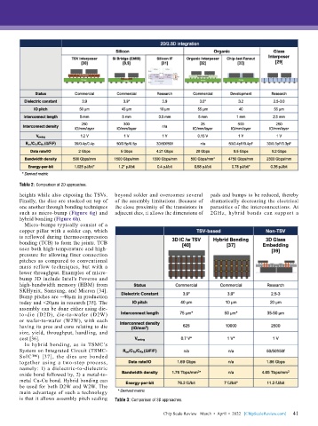
Table 2: Comparison of 2D approaches.
        heights while also exposing the TSVs.   beyond solder and overcomes several   pads and bumps to be reduced, thereby
        Finally, the dies are stacked on top of   of the assembly limitations. Because of   dramatically decreasing the electrical
        one another through bonding techniques   the close proximity of the transistors in   parasitics of the interconnections. At
        such as micro-bump (Figure 6g) and   adjacent dies, it allows the dimensions of   2GHz, hybrid bonds can support a
        hybrid bonding (Figure 6h).
          Micro-bumps typically consist of a
        copper pillar with a solder cap, which
        is reflowed during thermocompression
        bonding (TCB) to form the joints. TCB
        uses both high-temperature and high-
        pressure for allowing finer connection
        pitches as compared to conventional
        mass ref low techniques, but with a
        lower throughput. Examples of micro-
        bump 3D include Intel’s Foveros and
        high-bandwidth memory (HBM) from
        SKHynix, Samsung, and Micron [34].
        Bump pitches are ~40µm in production
        today and <20µm in research [35]. The
        assembly can be done either using die-
        to-die (D2D), die-to-wafer (D2W)
        or wafer-to-wafer (W2W), with each
        having its pros and cons relating to die
        size, yield, throughput, handling, and
        cost [36].
          In hybrid bonding, as in TSMC’s
        System on Integrated Circuit (TSMC-
        SoIC™) [37], the dies are bonded
        together  using a two-step process,
        namely: 1) a dielectric-to-dielectric
        oxide bond followed by, 2) a metal-to-
        metal Cu-Cu bond. Hybrid bonding can
        be used for both D2W and W2W. The
        main advantage of such a technology
        is that it allows assembly pitch scaling   Table 3: Comparison of 3D approaches.

                                                                                                             41
                                                             Chip Scale Review   March  •  April  •  2022   [ChipScaleReview.com]  41

