Page 46 - Chip Scale Review_March April_2022-digital
P. 46
capacitors are necessary. Unlike capacitors,   As multiple dies are assembled and   for silicon, or warpage and nonplanarity-
        inductors require a larger footprint and   connected, the size of the interposer is   related issues for organics. We believe that
        therefore, their integration in the interposer   bound to increase. The current trend in   future interposers would require larger sizes
                                                                                        2
        becomes necessary using magnetic materials   advanced packaging is towards supporting   of 10000mm  that can support fine-L/S of
        [43]. Along with magnetic material selection   high interconnection density using fine-L/S   1µm or less. As package sizes increase, the
        and process development, the design and   (<1µm) and increasing pin count to support   dimensional stability of the substrate and
        integration of these inductors pose unique   power delivery requirements. However, the   CTE of the substrate need to be carefully
        challenges that require significant co-design   maximum interposer size is restricted to   chosen to manage wafer/panel warpage
                                                  2
        effort between the die and interposer.  3000mm —either limited by reticle size   during processing. Panel-scale processing
                                                                              (on glass or organics) is seen as a path
                                                                              forward for cost-efficient scaling of the
                                                                              interposer size. Such processes today are
                                                                              limited to display technologies (glass) and
                                                                              low-IO count analog device manufacturing
                                                                              (laminates and panel fan out). Large-
                                                                              area lithography, precision deposition and
                                                                              etching tooling are needed to take this to
                                                                              high-volume manufacturing.
                                                                                As neural networks (NNs) become more
                                                                              complex, increasing bandwidth density
                                                                              and reducing latency require connectivity
                                                                              between interposers through the package
                                                                              substrate. In such scenarios, optical IOs in
                                                                              the interposer and optical waveguides in
                                                                              the package substrate become necessary
                                                                              for communication over longer distances
                                                                              through serialization of data. SerDes is an
                                                                              option for supporting such functionality.
                                                                              However, SerDes-based approaches
                                                                              are not energy efficient because the
                                                                              EPB is around 23pJ/bit for transmission
                                                                              distances of ~1cm with data rates of
                                                                              40Gb/s/lane (a bit error rate [BER] of
                                                                              10 ). An energy-efficient solution is the
                                                                                -9
                                                                              use of optical waveguides integrated
                                                                              into the package substrate coupled to


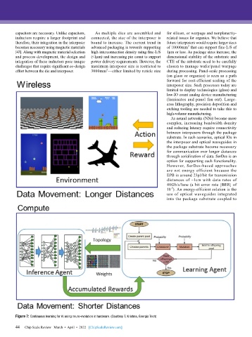
        Figure 7: Continuous learning for AI using neuro-evolution in hardware. (Courtesy T. Krishna, Georgia Tech)

        44   Chip Scale Review   March  •  April  •  2022   [ChipScaleReview.com]
        44

