Page 51 - Chip Scale Review_March April_2022-digital
P. 51
Wafer-level polymer/metal hybrid bonding using a


        photosensitive permanent bonding material


        By Baron Huang, Mei Dong, Shelly Fowler, Andrea Chacko, Rama Puligadda  [Brewer Science, Inc.]
        D          ownscaling is a never-


                   e n d i n g t a s k f o r
                   t he  s e m i c o nd u c t o r
        industry to meet the ever-increasing
        electronic system demands for higher
        performance and functionality, smaller
        system form factor, and lower power
        consumption and cost. Moore’s Law
        drove the industry for decades to
        double the number of transistors on a
        chip with node scaling for 2D device
        fabrication. However, the development
        of next-ge ne r at ion si l icon node
        manufacturing becomes more and
        more challenging and costly because of
        lithography limitations.
          Syst e m sca l i ng for 3D dev ice
        fabrication is an emerging concept
        for  i nt eg r at i ng  more  f u nct ion al
        m a t e r i a l s a l o ng w i t h va r i ou s
        semiconductor technologies in a chip,
        or more chip carrier packages stacked
        through advanced packaging and
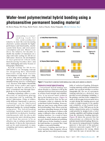
        manufacturing process technologies   Figure 1: Process flow for wafer-level hybrid bonding using a) oxide, and b) polymer as a dielectric.
        [1-2]. Devices with higher bandwidth
        and with better power and signal   Dielectric/metal hybrid bonding    fields of wafer-level bonding. Polymeric
        integrity can then be achieved in a   Conventional hybrid bonding uses   bonding materials exhibit good bond-line
        more economical way through finer-  silicon dioxide as a dielectric to fill up the   quality and excellent tolerance to surface
        pitch die-to-die interconnection.  interspace between micro-interconnections   topography [4]. The use of a polymeric
          Bonding technology offers a z-axis   to enhance bond strength and reliability.   bonding material as a dielectric layer
        d i rect ion of i nteg rat ion play i ng   Also, it can prevent metal oxidation   provides several advantages including: 1)
        an  important  role  in  realizing 3D   during the bonding process. Figure 1a   the polymer can flow better compared to
        device fabrication. Chips or wafers   illustrates the process flow for the use   oxide to fill air gaps between metal wires
        with different functional or process   of inorganic oxide as a dielectric for the   or pads during the bonding process and
        t e c h n o l o g y c a n b e f a b r i c a t e d   oxide/metal hybrid bonding. However,   results in improvements to the quality
        separately and then st acked and   there are some issues using silicon oxide   and reliability of the bonded stack.
        integrated together by vertical bonding   for hybrid bonding. First, silicon oxide has   Additionally, 2) the CMP process for the
        integ ration. T he hybr id bonding   poor stress absorption because of its high   surface planarization prior to bonding
        technology, based on metal-to-metal   modulus and the hardness of silicon oxide   could possibly be skipped with a better
        and dielectric-to-dielectric bonding   makes it difficult to flow or deform in the   bonding capability and bonding strength
        simultaneously with the die-to-die   bonding interface. As a result of these   from the polymeric bonding material.
        interconnection pitch shrinking down   challenges, using silicon oxide requires   Figure 1b shows the process flow for
        to  sub-10μm  has  proven  to  be  an   an extra chemical mechanical polishing   using polymer as a dielectric for the
        effective way to enhance performance   (CMP) process before bonding to ensure   polymer/metal hybrid bonding. However,
        and density of die-to-die interconnects   the bond interface is extremely flat (~1nm)   the concern for using polymeric bonding
        and can be used extensively in many   to achieve a successful bonding.  material is that most of the polymer
        computing and memory applications in   Polymeric bonding material has a   dielectric materials require 300°C or
        the future [3].                    lower modulus than inorganic silicon   higher temperature for curing, which
                                           oxide, and has been widely used in many   will limit the type of metals that can


                                                                                                             49
                                                             Chip Scale Review   March  •  April  •  2022   [ChipScaleReview.com]  49

