Page 53 - Chip Scale Review_March April_2022-digital
P. 53
a 5μm-thick film of the PS PBM was spin-coated onto a 100mm
                                                             wafer. The wafers were contact-baked on hot plates at 60°C for
                                                             5 minutes and 120°C for an additional 10 minutes for soft bake.
                                                             Exposure was conducted by an i-line mask aligner at an exposure
                                                             energy of 100mJ/cm . The wafer was then developed using a
                                                                              2
                                                             puddle develop process with cyclopentanone as the developer.
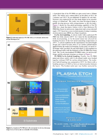
                                                             Figure 3 shows the fine-pitch patterning capability of the PS
                                                             PBM for a 4μm line/space feature with a 5μm thickness PS
                                                             PBM film (based on microscope inspection) and a steep sidewall
                                                             angle (~90°) based on a cross-section measured using a scanning
                                                             electron microscope (SEM) on a 10μm via pattern.
                                                               Cu-Sn electroplating. A silicon wafer with a patterned PS
                                                             PBM was fully cured at 200°C for 1 hour for the metallization
        Figure 3: Patterning capability of PS PBM: with a) a microscope; and b) cross-
        section SEM inspections.                             with electroplating. A Cu-Sn metal stack was selected for
                                                             bonding because of the low metal annealing temperature at
                                                             250°C. A critical condition for the experiment is the metal height
                                                             design and control because there is no surface planarization
                                                             applied before the wafer-level bonding. In this study, we used Cu-
                                                             Sn bumps with 2μm-thick Sn and 4μm-thick Cu electroplated on
                                                             the patterned wafer with the thickness of the PS PBM film being
                                                             5μm. The Cu-Sn electroplated PS PBM wafer, its microscope
                                                             image, and the schematic structure are shown in Figure 4.
                                                               PS PBM/Cu-Sn hybrid bonding. Finally, two PS PBM
                                                             patterned silicon wafers with Cu-Sn plated metals were bonded
                                                             together without CMP for surface planarization. The wafer-
                                                             level hybrid bonding was conducted at 250°C for 60min with a
                                                             bonding pressure of 20kN to form an interconnection between
                                                             the layers. The bonded wafer pair was further analyzed by


        Figure 4: a) A patterned PS PBM wafer with electroplated Cu-Sn; b) a microscope
        image of a Cu-Sn bump; and c) a schematic of the structure.

                                                                                                             51
                                                             Chip Scale Review   March  •  April  •  2022   [ChipScaleReview.com]  51

