Page 56 - Chip Scale Review_March April_2022-digital
P. 56
Enabling low-profile LSCs for automotive


        flip-chip packaging


        By Jaimal Williamson, David Chin  [Texas Instruments]
        L        and-side capacitors (LSCs)   as compared to DSCs (i.e., based on   of both component- and board-level


                 are vit al semiconductor
                 p a ck a g i n g  c o m p o n e nt s   the aforementioned keep out zone   mea su reme nt s bet wee n t he LSC
                                                                              and the collapsed BGA solder ball
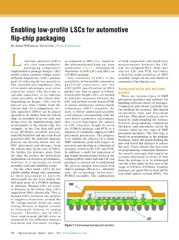
                                           constraints). Figure 1 showcases an
        implemented in package designs. LSCs   illustration of both LSCs and DSCs on   and the LSC and PCB, facilitates
        enable a more constant voltage across   a FCBGA package.              a detailed understanding of  SMT
        different frequencies, with a primary   O ne li m it at ion of LSCs is t he   assembly margin for the safe launch of
        goal of reducing device parasitics   availability of low-profile automotive   automotive flip-chip devices.
        like crosstalk and impedance. One   q u a l i f i e d c a p a c i t o r s p e r t h e
        of its main advantages over other   AEC- Q200 specif ication at BGA   Background on the pick and place
        capacitor t y pes, like die-side or   pitches less than or equal to 0.8mm.   process
        top-side capacitors, is its inherent   Low-profile height LSCs are needed   There are various types of SMT
        closer proximity to the silicon chip.   to maintain clearance between the   placement machines and software for
        Depending on design, LSCs can be   LSC and printed circuit board (PCB)   handling different classes of packages.
        placed less than 1.0mm from the    to ensure satisfactory surface mount   Component placement typically has
        silicon chip. As a comparison, die-  tech nolog y (SM T ) a ssembly. As   two methods for accuracy  that depend
        side capacitors (DSCs) can be placed   such, to better understand assembly   on ma ch i ne t y pe a nd pla cement
        upwards to 4x farther from the silicon   yield margin corresponding with the   software. Placement accuracy can be
        chip, as assembly keep out zone and   zero-defect automotive requirement,   honed by understanding the balance
        design rules for manufacturing limit   this review highlights the impact   between programming component
        its proximity to the silicon chip. For   of LSC clearance height between   thickness and placement speed. In
        example, in the f lip-chip  ball grid   the FCBGA package and PCB as a   essence, there are two types of SMT
        array (FCBGA) assembly process,    function of commonly employed SMT   placement machines. The first type is
        underfill backflow and any resin bleed   placement parameters. The purpose   based on programming in the package
        generated after the underfill dispense   is to validate the efficacy of a robust   thickness, where the nozzle holding the
        process can directly factor into the   SMT continuity yield with respect to   part will travel that distance to release
        DSC placement and distance from    non-wets and shorting as a function of   the part. Users choose the first type
        the silicon chip. In the case of DSCs,   clearance between the LSC and PCB.   of programming component thickness
        the farther the distance away from   In addition, a multi-lot inspection of   for specific packages that require an
        the chip, the greater the deleterious   gap height measurements between the   accurate placement in terms of how
        implications on electrical performance,   collapsed BGA solder ball and LSC (on   deep the package is to be submerged
        however, it is necessar y to avoid   package) is carried out to understand   into the solder paste (in this case in the
        assembly yield and reliability issues.  the process margin associated with   range of 0.05mm–0.075mm). Example
          On the other hand, LSCs do not   chip-to-package effects (i.e., substrate   packages are quad flat no-lead (QFN)
        exhibit similar design rule constraints   size, die-to-package ratio) post-  and small outline no-lead (SON). The
        a s  t h e i r p l a c e m e n t i s  d i r e c t l y   FCBGA assembly. The combination
        underneath the die area within the
        ball grid array of a FCBGA package
        or substrate. Because LSCs are closer
        in distance to the silicon chip, LSCs
        outperform DSCs electrically. This is
        because LSCs minimize any positive
        or negative excursions around the
        DC voltage (noise), which can cause
        timing failures in digital circuits
        or f u nct ional failu res i n a nalog
        circuits. Therefore, use of LSCs
        lower peak-to-peak (pk2pk) noise as
        measured by the difference between
        minimum and maximum voltages
                                           Figure 1: FCBGA package illustrating LSCs and DSCs.

        54   Chip Scale Review   March  •  April  •  2022   [ChipScaleReview.com]
        54

