
Page 54 - Chip Scale Review_March April_2022-digital
P. 54
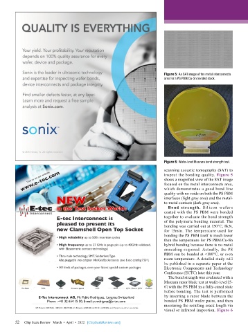
Figure 5: An SAT image of the metal interconnects
                                                                              area for a PS PBM/Cu-Sn bonded stack.


                                                                              Figure 6: Wafer-level Maszara bond strength test.
                                                                              scanning acoustic tomography (SAT) to
                                                                              inspect the bonding quality. Figure 5
                                                                              shows a magnified view of the SAT image
                                                                              focused on the metal interconnects area,
                                                                              which demonstrates a good bond line
                                                                              quality with no voids on both the PS PBM
                                                                              interfaces (light gray area) and the metal-
                                                                              to-metal contacts (dark gray area).
                                                                                Bond strength. Silicon wafers
                                                                              coated with the PS PBM were bonded
                                                                              together to evaluate the bond strength
                                                                              of the polymeric bonding material. The
                                                                              bonding was carried out at 150°C, 8kN,
                                                                              for 15min. The temperature used for
                                                                              bonding the PS PBM itself is much lower
                                                                              than the temperature for PS PBM/Cu-Sn
                                                                              hybrid bonding because there is no metal
                                                                              annealing required. Actually, the PS
                                                                              PBM can be bonded at <100°C, or even
                                                                              room temperature. A detailed study will
                                                                              be published in a separate paper at the
                                                                              Electronic Components and Technology
                                                                              Conference (ECTC) later this year.
                                                                                The bond strength was evaluated with a
                                                                              Maszara razor blade test at wafer-level [5-
                                                                              6] with the PS PBM in a fully-cured state
                                                                              before bonding. The test is performed
                   E-Tec Interconnect  AG, Mr. Pablo Rodriguez,  Lengnau Switzerland  by inserting a razor blade between the
                       Phone : +41 32 654 15 50, E-mail: p.rodriguez@e-tec.com  bonded PS PBM wafer pairs, and then
                                                                              measuring the resulting crack length via
                                                                              visual or infrared inspection. Figure 6

        52
        52   Chip Scale Review   March  •  April  •  2022   [ChipScaleReview.com]