Page 58 - Chip Scale Review_March April_2022-digital
P. 58
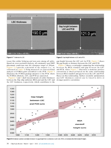
Figure 4: Thickness of a LSC.                        Figure 5: Gap height between a LSC and a PCB.

        issues like solder bridging and non-wets among all splits.  gap height between the LSC and the PCB. Figure 5 shows
        Based on cross-sectional analysis, all commonly used SMT  the gap height or distance between the LSC and PCB.
        placement conditions met the clearance target of 100µm.   Figure 6 shows a scatterplot comparing the relationship
        Figure 2-4 provide a pictorial of the outputs (i.e., as  between the BGA standoff and gap between the LSC
        referenced in Table 1) being measured via cross-sectional  and PCB, where Figure 7 illustrates a moderate positive
        analysis of FCBGA parts assembled to the PCB. Figure 2  correlation is observed based on the same relationship
        illustrates the FCBGA package mounted to the PCB, where  between BGA standoff and gap between the LSC and PCB.
        the FCBGA substrate, LSC, and PCB are annotated.     Based on this relationship, further assembly optimization
          Figures 3 and 4 show measurements of solder thickness  and LSC thickness control can be tuned to drive at
        between the flip-chip substrate BGA pad and the LSC and  stronger positive correlation.
        the LSC thickness, respectively, which contributes to the


        Figure 6: Moderate positive correlation between the gap height that is between an LSC and a PCB, and between the BGA standoff height.

        56
        56   Chip Scale Review   March  •  April  •  2022   [ChipScaleReview.com]

