Page 61 - Chip Scale Review_March April_2022-digital
P. 61

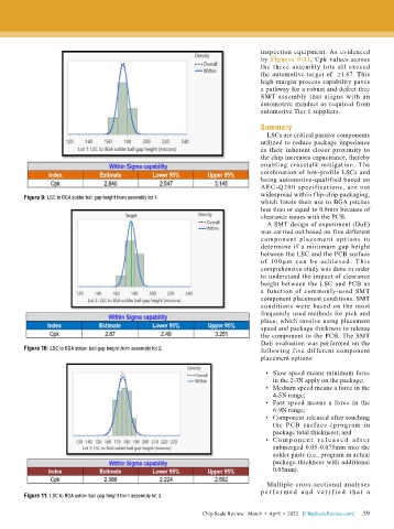
inspection equipment. As evidenced
                                                                              by Figures 9-11, Cpk values across
                                                                              the three assembly lots all exceed
                                                                              the automotive target of  ≥1.67. This
                                                                              high-margin process capability paves
                                                                              a pathway for a robust and defect-free
                                                                              SMT assembly that aligns with an
                                                                              automotive mindset as required from
                                                                              automotive Tier 1 suppliers.

                                                                              Summary
                                                                                LSCs are critical passive components
                                                                              utilized to reduce package impedance
                                                                              as their inherent closer proximity to
                                                                              the chip increases capacitance, thereby
                                                                              enabling crosstalk mitigation. The
                                                                              combination of low-profile LSCs and
                                                                              being automotive-qualified based on
                                                                              AEC-Q200 specifications, are not
                                                                              widespread within flip-chip packaging,
        Figure 9: LSC to BGA solder ball gap height from assembly lot 1.
                                                                              which limits their use to BGA pitches
                                                                              less than or equal to 0.8mm because of
                                                                              clearance issues with the PCB.
                                                                                A SMT design of experiment (DoE)
                                                                              was carried out based on five different
                                                                              component placement options to
                                                                              determine if a minimum gap height
                                                                              between the LSC and the PCB surface
                                                                              of  100µm  can  be  achieved.  T his
                                                                              comprehensive study was done in order
                                                                              to understand the impact of clearance
                                                                              height between the LSC and PCB as
                                                                              a function of commonly-used SMT
                                                                              component placement conditions. SMT
                                                                              conditions  were based  on  the  most
                                                                              frequently used methods for pick and
                                                                              place, which involve using placement
                                                                              speed and package thickness to release
                                                                              the component to the PCB. The SMT
                                                                              DoE evaluation was performed on the
        Figure 10: LSC to BGA solder ball gap height from assembly lot 2.     following five different  component
                                                                              placement options:

                                                                                •  Slow speed means minimum force
                                                                                  in the 2-3N apply on the package;
                                                                                •  Medium speed means a force in the
                                                                                  4-5N range;
                                                                                •  Fast speed means a force in the
                                                                                  6-9N range;
                                                                                •  Component released after touching
                                                                                  the PCB surface ( program in
                                                                                  package total thickness); and
                                                                                •  C o m p o n e n t r e l e a s e d  a f t e r
                                                                                  submerged 0.05-0.075mm into the
                                                                                  solder paste (i.e., program in actual
                                                                                  package thickness with additional
                                                                                  0.05mm).

                                                                                Multiple cross-sectional analyses
                                                                              p e r f o r m e d a n d v e r i f i e d t h a t  a
        Figure 11: LSC to BGA solder ball gap height from assembly lot 3.

                                                                                                             59
                                                             Chip Scale Review   March  •  April  •  2022   [ChipScaleReview.com]  59
   56   57   58   59   60   61   62   63   64