Page 57 - Chip Scale Review_March April_2022-digital
P. 57
disadvantages of this approach are
        the slower speed of placement, and an
        additional step to measure the package
        thickness during programming.
          T he second t y pe of placement
        machine is based on using force to
        release the device onto the PCB. The
        nozzle holding the device carries the
        component until it touches the PCB
        surface with a reaction force. With
        respect to SMT assembly, placement
        force is associated with placement
        speed. The aforementioned method of
        using force (placement speed) is more
        common because users simply need
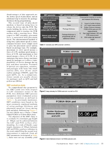
        to pick the placement speed option   Table 1: Commonly used SMT placement conditions.
        based on package type. For example,
        minimum or slow speed means a
        force of 2-3N, medium speed means a
        force of 4-5N, and maximum or fast
        speed means a force of 6-9N. It is
        customary that users choose maximum
        speed for packages as it offers a lower
        possibility of device damage during
        pick and place  operation. Examples
        of devices are capacitors, resistors,
        and packages with leads like small
        out l i ne (SO), t h i n sh r i n k sm a l l
        outline package (TSSOP), quad flat
        pack (QFP), etc. As a comparison,
        slower speeds are usually chosen
        for packages such as QFN and ball
        grid arrays (BGAs).

        SMT evaluation study
          To comprehend any propensit y
        for SMT yield loss with respect
        t o L SC cle a r a n c e  i s s u e s t o t h e   Figure 2: Image showing the FCBGA substrate mounted to a PCB.
        PCB, f ive different SMT process
        parameters were evaluated across
        var ious conditions as def ined in
        Table 1. As previously mentioned,
        SMT conditions were based on the
        most commonly employed methods
        of u si ng pa ck age t h ick ne ss a nd
        placement speed (or force) during
        pick and place. Referencing Figure 1,
        the test vehicle was a 24mm x 24mm
        lidded FCBGA at 0.8mm BGA pitch.
          The objective of the SMT study is
        to evaluate if a minimum gap height
        of  100µm can be achieved between
        t he  LSC  a nd  PC B  s u r fa c e  a f t e r
        mounting. As a rule of thumb, a gap
        height clearance of 100µm between
        LSC and PCB is used as a reference in
        the event underfilling the second level
        interconnect is required. From all
        SMT parameters investigated in Table
        1, there were not any assembly yield
                                           Figure 3: Solder thickness between the FCBGA pad and a LSC.

                                                                                                             55
                                                             Chip Scale Review   March  •  April  •  2022   [ChipScaleReview.com]  55

