Page 37 - Chip Scale Review_March April_2022-digital
P. 37
Heterogeneous integration for AI applications: status


        and future needs (part 2)


        By Madhavan Swaminathan, Siddharth Ravichandran  [Georgia Institute of Technology]

        Part 1 of this article was published in the January/February 2022 issue of Chip Scale Review.
        I     n part 1 of this article, the


              emerging artificial intelligence
              (AI) system needs that are driving
        various packaging architectures were
        discussed along with 7 metrics driving
        new technologies. These metrics include
        interconnect density, interconnect length,
        data rate, bandwidth density, energy per
        bit, power delivery, and thermal design
        power. In part 2, we compare the state-of-
        the-art (SOTA) packaging technologies
        based on these metrics along with future
        requirements. [Note to readers: figure and
        reference numbers start where numbering
        left off in part 1.]

        Packaging, interposers, and 3D
        stacking options
          In this section we refer to high-density
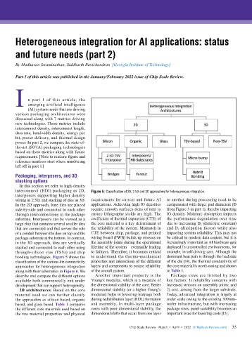
        interconnect (HDI) packaging as 2D,   Figure 5: Classification of 2D, 2.5D and 3D approaches for heterogeneous integration.
        interposers supporting higher density
        wiring as 2.5D, and stacking of dies as 3D.   requirements for current and future AI   to another during processing need to be
        In the 2D approach, bare dies are placed   applications. Achieving high IO densities   compensated with larger pad diameters (D
        side-by-side and connected to each other   require smooth surfaces (tens of nm) to   from Figure 3 in part 1), thereby impacting
        through interconnections in the package   ensure lithography yields are high. The   IO density. Moisture absorption impacts
        substrate. Interposers can be viewed as a   coefficient of thermal expansion (CTE) of   the performance degradation over time
        large chip that contains several smaller dies   the core material is a key determinant of   due to increasing D k  (dielectric constant)
        that are connected and that serves the role   the reliability of the system. Mismatch in   and D f  (dissipation factor) while also
        of a conduit between the dies on top and the   CTE between chip, package, and printed   impacting system reliability. This may not
        package substrate at the bottom. In contrast,   wiring board (PWB) builds up stresses on   be critical in modern data centers, but it is
        in the 3D approach, dies are vertically   the assembly joints during the operational   increasingly important as AI hardware gets
        stacked and connected to each other using   lifetime of the system—eventually leading   deployed in uncontrolled environments, for
        through-silicon vias (TSVs) and chip   to failures. Therefore, it becomes critical   example, in self-driving cars. Although the
        bonding technologies. Figure 5 shows the   to understand the thermo-mechanical   dominant heat path is through the backside
        classification of the various die connectivity   properties and interactions of the different   of the die [14], the thermal conductivity of
        approaches for heterogeneous integration   layers and components to ensure reliability   the core material is worth noting and shown
        along with their schematics in Figure 6. We   of the overall system.   in Table 1.
        describe and compare the different options   Another important property is the   Package  sizes  are  limited by  two
        available both commercially and under   Young’s modulus, which is a measure of   key factors: 1) reliability concerns with
        development that can support heterogeneity.  the dimensional stability of the core. Better   increased stresses on assembly joints; and
          2D architectures. Based on the core   dimensional stability (or a higher Young’s   2) cost, arising from the larger substrate.
        material used we can further classify   modulus) helps in lowering warpage both   Today, advanced integration is largely at
        the approaches as silicon based, organic   during redistribution layer (RDL) formation   wafer scale owing to the existing 300mm-
        based, and glass based. Table 1 compares   and assembly. In multi-layer package   wafer infrastructure, but with increasing
        the different core materials used based on   cores with poor dimensional stability, the   package sizes, panel scalability becomes an
        the raw material properties and physical   dimensional shifts that occur from one layer   important issue for lowering costs [15].


                                                                                                             35
                                                             Chip Scale Review   March  •  April  •  2022   [ChipScaleReview.com]  35

