Page 29 - Chip Scale Review_March April_2022-digital
P. 29
Embedded chip packaging


        By Ray Fillion  [Fillion Consulting]

        I     n the November/December 2021


              issue of Chip Scale Review, seven
              advanced packaging technologies
        were described [1]. The article covered
        embedded chip packaging (ECP), fan-in
        wafer-level packaging (FIWLP), fan-out
        wafer-level and panel-level packaging
        (FOWLP, FOPLP), 3D packaging and
        system-in-package (SiP) and compared
        how well each meets the basic functions
        of microelectronics packaging. In this
        article, we will go into a more in-depth
        look at ECP, detailing the structures,
        processes and  materials used  in the
        various versions of ECP technologies and
        look at some of the unusual application
        areas where ECP is being applied.

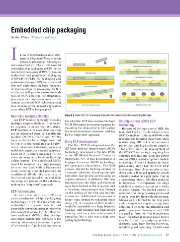
        Multichip modules (MCMs)           Figure 1: Basic COF ECP processing steps with two overlay layers interconnecting the chips.
          An ECP module typically includes   the substrate. ECP also reverses the basic   GE chip-on-flex (COF) ECP
        multiple chips embedded in or under   MCM fabrication processing sequence by
        an organic interconnect structure.   mounting the chips prior to fabricating   technology
        ECP modules with more than one chip   the interconnection structure, making   Because of the high cost of HDI, the
        are an advanced form of a multichip   ECP a “chips-first” approach.   team that I led at GE developed a new
        module (MCM). Traditional MCMs                                        ECP technology in the mid-1990s with
        have multiple bare chips mounted   Early ECP development              modifications targeting lower costs while
        on top of a pre-fabricated and fully-  The first ECP development was the   maintaining HDI’s low interconnect
        tested interconnect structure, such as a   GE high-density interconnect (HDI)   parasitics  and  high  silicon density.
        multilayer organic or ceramic substrate.   technology developed in the late 1980s   This effort led to the development of
        Each chip is interconnected to the   at the GE Global Research Center in   the GE COF technology, targeting less
        substrate using wire bonds or flip-chip   Niskayuna, NY. It was developed as a   complex modules and later, the power
        solder bumps. The completed MCM    high-performance MCM technology    overlay (POL) embedded power module
        would be mounted in a large package   for aerospace electronics. The HDI   technology. Figure 1 depicts the basic
        or over molded with a ther moset   process started by forming cavities in   processing steps for the COF ECP
        resin, creating a molded package. In   a ceramic substrate, attaching multiple   technology. Bare chips are placed face
        traditional MCMs, the substrate is   bare chips face up into cavities using an   down onto a B-staged (partially-cured)
        fabricated and tested first, and then   organic adhesive. A dielectric film was   adhesive coated on a polyimide film on
        the chips are placed on the substrate,   laminated over the chips and microvias   a processing platen. Molding material
        making it a “chips-last” approach.  were laser-formed to the chip pads and   is dispensed to encapsulate the chips
                                                                              and form a molded carrier in a wafer
                                           a fine-line interconnect was formed   or panel format. The molded carrier is
        ECP technologies                   on the surface of the film and into the   removed from the processing platen and
          As the ter m i mplies, ECP is a   microvias. Additional interconnect   flipped over for front-side processing.
        s e m i c o n d u c t o r c h i p p a c k a g i n g   layers were formed by repeating these   Microvias are formed to the chip pads
        technology in which bare chips are   steps [2]. A completed HDI module   and to component contacts using laser
        embedded in organic material and   would be assembled in a large hermetic   ablation. The same metallization and
        electrically connected using an overlying   package. HDI modules had high silicon   pattern processes developed with HDI
        interconnect structure. ECP MCMs differ   density and very low interconnect   are used to form the first interconnect
        from traditional MCMs in that the chips   parasitics, but it also was a high-cost   layer. Additional interconnect layers
        have direct metallurgical connects to the   packaging technology.     can be formed by applying another
        overlay interconnect structure in place                               dielectric layer, laser-forming microvias,
        of wire bond or flip-chip connections to                              metallizing and patterning. As with most


                                                                                                             27
                                                             Chip Scale Review   March  •  April  •  2022   [ChipScaleReview.com]  27

