Page 25 - Chip Scale Review_March April_2022-digital
P. 25
41% from the 6L RDL to the 1L RDL
        case, individually. Therefore, the
        simulation result shows that the chip-
        last structure has a lower stress effect
        on the top RDL layer because the under
        fill functions as a strong buffer layer
        that absorbs the stress from the corner
        area of the top die. What this means is,
        the FO-MCM structure — by using the
        chip-last process — has a lower risk of
        RDL cracking because of the protection
        provided by the under-fill layer.

        Warpage measurement results
          Generally, the biggest challenge
        for FO packaging is warpage control
        because if mismanaged, it can be
        an inter r uption. This situation is
        particularly challenging for finer
        high-density FO-RDL used in multi-
        die integration. A larger package size
        and more RDL layers are the factors
        that result in severe warpage and yield
        loss. In this study, we obtained yield
        results using a wafer with 2/2µm L/
        S RDL in chip-first and chip-last
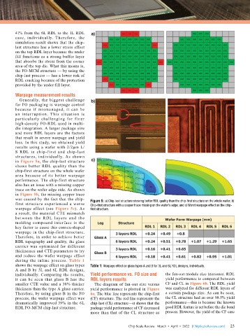
        structures, individually. As shown
        in Figure 5a, the chip-last structure
        shows better RDL quality than the
        chip-first structure on the whole wafer
        area because  of  its better  warpage
        performance. The chip-first structure
        also has an issue with a missing copper
        trace on the wafer edge side. As shown
        in Figure 5b, the missing copper trace
        was caused by the fact that the chip-  Figure 5: a) Chip-last structure showing better RDL quality than the chip-first structure on the whole wafer; b)
        first structure experienced a worse   Chip-first structure with a copper trace missing on the wafer’s edge; and c) Worst warpage effect on the chip-
        warpage effect (see  Figure 5c). As   first structure.
        a result, the material CTE mismatch
        bet ween the R DL layers and the
        molding compound interface is the
        key factor to cause this convex-shaped
        warpage in the chip-first structure.
        Therefore, in order to achieve better
        RDL topography and quality, the glass
        carrier was optimized for different
        thicknesses and CTE parameters to try
        and reduce the wafer warpage effect
        during the inline process.  Table 1
        shows the warpage effect on glass types   Table 1: Warpage effect on glass types A and B for 3L and 6L RDL designs, individually.
        A and B by 3L and 6L RDL designs,
        individually. Comparing the results,   Yield performance vs. FO size and   the fan-out module size increases. RDL
        it  can  be  seen  that  glass  B  has  the   RDL layers results      yield performance is compared between
        smaller CTE value and a 30% thicker   The diagram of fan-out size versus   CF and CL in Figure 6b. The RDL yield
        thickness than the type A glass carrier.   yield performance is plotted in Figure   was analyzed for different RDL layers of
        Therefore, by using glass B in the FO   6a. The blue line represents the chip-first   a certain package size. As can be seen,
        process, the wafer warpage effect was   (CF) structure. The red line represents the   the CL structure had an over 98.5% yield
        dramatically improved 39% in the 6L   chip-last (CL) structure—it shows that the   performance—this is because the known
        RDL FO-MCM chip-last structure.    package yield performance of CF decreased   good RDL feature is set before the die bond
                                           more than that of the CL structure as   process. However, the yield of the CF case


                                                                                                             23
                                                             Chip Scale Review   March  •  April  •  2022   [ChipScaleReview.com]  23

