Page 22 - Chip Scale Review_March April_2022-digital
P. 22
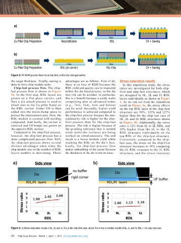
Figure 3: FO-MCM process flows for a) chip-first, and b) chip-last approaches.
        the target thickness.  Finally, sawing is   advantages are as follows. First of all,   Stress simulation results
        done to form chip module units.    there is no loss of KGD because the   In this simulation study, the stress
          Chip-last process flow. The chip-  RDL yield and quality can be inspected   ratios are investigated for both chip-
        last process flow is shown in Figure   before the die bond process, so the die   first and chip-last structures, which
        3b. In the first step, RDL layers are   loss risk can be avoided. In particular,   are designed by 6L, 2L and 1L RDL
        grown on a f lat glass carrier, and   this is a benefit because a costly wafer   layers individually as shown in Figure
        then a die attach process is used to   comprising dies at advanced nodes   4. As we can see from the simulation
        attach dies to the Cu pillar bump on   (e.g., 7nm, 5nm, 3nm and below)   result in Figure 4a, the stress effects
        the RDL carrier. Under fill is then   can be used. Secondly, higher yield   on the top RDL layer of the chip-first
        added into the micro-bump space to   performance is achieved compared to   structure are 90%, 119% and 127%
        protect the interconnect area. Next, the   the chip-first process because the non-  higher than for the chip-last case of
        RDL module is covered with molding   coplanarity risk is higher for the chip-  6L, 2L and 1L RDL structures shown
        compound. And lastly, the carrier is   first process than for the chip-last   in Figure 4b. Additionally, the stress
        removed and C4 bumps are grown on   process. The risk is higher because of   ratio is 12% from 6L to 2L RDL, and
        the opposite RDL surface.          the grinding tolerance that is needed   18% higher from the 6L to the 1L
          Compared to the chip-first process,   when multi-die surfaces are being   RDL structure individually on the
        however, the chip-last process has a   worked on simultaneously. The end   top RDL of the chip-last structure.
        more complicated process flow. Still,   result is a lower module yield while   Conversely, compared to the chip-
        the chip-last process shows several   stacking the RDL on the die’s face.   last case, the stress on the chip-first
        obvious advantages when either the   Lastly, the chip-last process f low   structure increases to 29% comparing
        chip module size or the number of RDL   makes embedding of die easier because   the 6L RDL structure to the 2L RDL
        layers  number  is  increasing.  Those   the thickness of the die is not an issue.  structure; and the stress increases


        Figure 4: a) Stress simulation results of 6L, 2L and 1L RDL in the chip-first case; and b) The stress simulation results of 6L, 2L and 1L RDL in the chip-last case.

        20   Chip Scale Review   March  •  April  •  2022   [ChipScaleReview.com]
        20

