Page 26 - Chip Scale Review_March April_2022-digital
P. 26
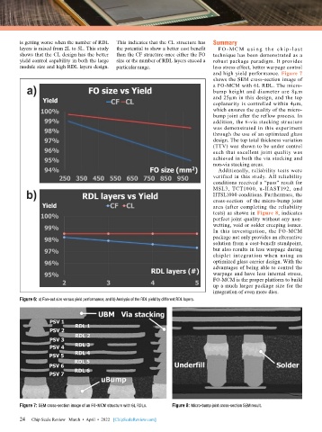
is getting worse when the number of RDL   This indicates that the CL structure has   Summary
        layers is raised from 2L to 5L. This study   the potential to show a better cost benefit   F O - M C M u s i n g t h e  c h i p - l a s t
        shows that the CL design has the better   than the CF structure once either the FO   technique has been demonstrated as a
        yield control capability in both the large   size or the number of RDL layers exceed a   robust package paradigm. It provides
        module size and high RDL layers design.   particular range.           less stress effect, better warpage control
                                                                              and high yield performance. Figure 7
                                                                              shows the SEM cross-section image of
                                                                              a FO-MCM with 6L RDL. The micro-
                                                                              bump height and diameter are 8µm
                                                                              and 25µm in this design, and the top
                                                                              coplanarity is controlled within 4µm,
                                                                              which ensures the quality of the micro-
                                                                              bump joint after the reflow process. In
                                                                              addition, the 6-via stacking structure
                                                                              was demonstrated in this experiment
                                                                              through the use of an optimized glass
                                                                              design. The top total thickness variation
                                                                              (TTV) was shown to be under control
                                                                              such that excellent joint quality was
                                                                              achieved in both the via stacking and
                                                                              non-via stacking areas.
                                                                                Additionally, reliability tests were
                                                                              verified in this study. All reliability
                                                                              conditions received a “pass” result for
                                                                              MSL3, TCT1000, u-HAST192, and
                                                                              HTSL1000 conditions. Furthermore, the
                                                                              cross-section  of the micro-bump joint
                                                                              area (after completing the reliability
                                                                              tests) as shown in Figure 8, indicates
                                                                              perfect joint quality without any non-
                                                                              wetting, void or solder creeping issues.
                                                                              In this investigation, the FO-MCM
                                                                              package not only provides an alternative
                                                                              solution from a cost-benefit standpoint,
                                                                              but also results in less warpage during
                                                                              chiplet integration when using an
                                                                              optimized glass carrier design. With the
                                                                              advantages of being able to control the
                                                                              warpage and have less internal stress,
                                                                              FO-MCM is the proper platform to build
                                                                              up a much larger package size for the
                                                                              integration of even more dies.
        Figure 6: a) Fan-out size versus yield performance; and b) Analysis of the RDL yield by different RDL layers.


        Figure 7: SEM cross-section image of an FO-MCM structure with 6L RDLs.  Figure 8: Micro-bump joint cross-section SEM result.

        24
        24   Chip Scale Review   March  •  April  •  2022   [ChipScaleReview.com]

