Page 19 - Chip Scale Review_March April_2022-digital
P. 19
Large-size multi-layered fan-out RDL multi-chip


        module packaging


        By Nicholas Kao, Jay Li, Jackson Li, Yu-Po Wang  [Siliconware Precision Industries Co., Ltd]
        I       Heterogeneous integration   tests, which are qualif ied in the   bandwidth requirement, while also


              is the key technology that is
              applied in high-performance   experiment, include: 1) temperature   enabling more effective die partitioning
                                                                              to shorten the time to market  [1-5].
                                           cycling testing (TCT) for  1000 cycles;
        c o m pu t i ng ( H P C ) , a r t i f i c i a l   2) unbiased highly-accelerated stress   However, the traditional monolithic
        intelligence (AI) and cloud computing   testing (u-HAST) for 192 hours; and 3)   die design in which a multi-core is
        applications, as well as for die-to-die   high-temperature storage life (HTSL)   integrated into one system on chip
        interconnections, application-specific   testing for 1000 hours. Undoubtedly,   (SoC) die architecture is facing many
        integrated circuits (ASICs) to high-  heterogeneous integration with multi-  challenges, such as increasing wafer
        bandwidth memory (HBM), and ASIC-  layer fan-out RDL is the mainstream   cost, limited die size, and high power
        to-ASIC. The higher I/O density, wider   for  AI, cloud  computing  and HBM   consumption. Consequently, fan-out
        data transmission bandwidth between   integration in the IC package industry.   packaging was proposed and developed
        memory to active die and lower RC   By utilizing this multi-layer RDL   as the robust solut ion to reduce
        delay are required in chiplet integration.   with compatible glass technology, the   packaging costs and provide a more
        Heterogeneous  integration  between   stability and yield of the fine-pitch die   flexible chiplet combination by using
        different functional dies, however,   bond will be improved.          die partition methodology. The resulting
        leads to various process challenges,                                  fan-out redistribution layer (FO-
        such as warpage control for multi-  Background                        RDL) technology became an essential
        layered redistribution layers (RDLs),   O v e r t h e l a s t  d e c a d e , t h e   routing technology between the die to
        surface co-planarization treatment,   s e m i c o nd u c t o r  i nd u s t r y  h a s   die interconnect area. Additionally,
        and solder joint capability during the   demonstrated the incredible possibilities   finer line/space (L/S) values of metal
        die bonding (DB) process. Therefore,   for  revolutionary  technologies.  For   trace and multi-layer RDL routing are
        in this article, we demonstrate a large   example,  several advanced packaging   required in order to enhance the high-
        size fan-out multi-chip module (FO-  technologies have been developed to   speed and demands for large-volume
        MCM) package with 6-layers of RDLs   accelerate machine learning (ML), AI   data processing.
        that successfully overcomes the non-  and HPC applications, such as 2.5D/3D,   Fa n - ou t t e c h n ol o g y h a s b e e n
        wetting issue and warpage effects   FO-MCM, fan-out embedded bridge   developed into a variety of structures
        by using optimized RDL technology   (FO-EB), and fan-out package-on-  for particular applications or purposes.
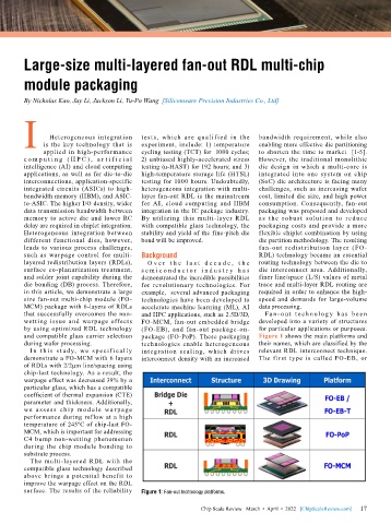
        and compatible glass carrier selection   package (FO-PoP). These packaging   Figure 1 shows the main platforms and
        during wafer processing.           technologies enable heterogeneous   their names, which are classified by the
          I n  t h is  st udy,  we  sp e ci f ical ly   integration  scaling,  which  drives   relevant RDL interconnect technique.
        demonstrate a FO-MCM with 6 layers   interconnect density with an increased   The first type is called FO-EB, or
        of RDLs with 2/2µm line/spacing using
        chip-last technology. As a result, the
        warpage effect was decreased 39% by a
        particular glass, which has a compatible
        coefficient of thermal expansion (CTE)
        parameter and thickness. Additionally,
        we  a ssess  ch ip  modu le  wa r page
        performance during reflow at a high
        temperature of 245ºC of chip-last FO-
        MCM, which is important for addressing
        C4 bump non-wetting phenomenon
        during the chip module bonding to
        substrate process.
          The  multi-layered  RDL  with  the
        compatible glass technology described
        above brings a potential benefit to
        improve the warpage effect on the RDL
        surface. The results of the reliability   Figure 1: Fan-out technology platforms.

                                                                                                             17
                                                             Chip Scale Review   March  •  April  •  2022   [ChipScaleReview.com]  17

